OSD335x C-SiP Design Tutorial
Published On: November, 29, 2018 By: Eshtaartha Basu | Updated: April 10, 2019 by Cathleen Wicks
The OSD335x C-SiP is a complete AM335x based System-in-Package (SiP) that integrates all the necessary components required for a typical embedded system. In addition to the 1GHz ARM Cortex© A8 processor, DDR memory, Power Management, EEPROM and passive components found in other members of the OSD335x Family, the OSD335x C-SiP also integrates up to 16GB eMMC Non-Volatile storage and MEMS Oscillator into a single package. It also features a ball map that allows designers to easily escape all signals in a single printed circuit board (PCB) layer.
This Tutorial Series consists of two lessons: OSD335x Reference Design Lessons 1 and 2. The OSD335x Lesson series is designed to help you quickly get started with OSD335x Family of devices and it mainly revolves around OSD335x-BAS. Since OSD335x-BAS and OSD335x C-SiP share many common features, most of the information provided in Lessons 1 and 2 for the BAS device also apply for the OSD335x C-SiP. This document will highlight the differences between OSD335x-BAS and OSD335x C-SiP that need to be considered during design process.
Lesson 1 covers:
- Introduction to Bare Minimum Circuitry to Boot OSD335x-SM
- Power Inputs and Outputs
- Ground Connections
- Power Management
- Clamping Circuit
- ESD Protection
- Reset Circuitry
- Clock Circuitry
- Peripheral Circuitry
- Bare Minimum Board Bring Up Process
Lesson 2 covers:
- Introduction to Bare Minimum Circuitry for Linux Boot
- USB Circuitry
- Adding Non-Volatile Storage
- Bringing Up a Custom Bare-Bones Linux PCB
- Linux Boot Process with the OSD335x
- Linux Device Tree
- Linux Device Tree Overlay
![]()
![]() A PDF version of this document can be found here.
A PDF version of this document can be found here.
Before You Begin
Fundamentals of the OSD335x C-SiP
There are a number of different parts within the OSD335x Family: OSD335x, OSD335x-SM, and OSD335x C-SiP (Please refer to the appropriate datasheet for specific orderable part numbers). In this document, we will be focusing on the OSD335x C-SiP (OSD3358-512M-BCB or OSD3358-512M-ICB) while making references to the OSD335x (OSD335x-512M-BAS) wherever necessary. All future references to the OSD335x C-SiP imply the (OSD3358-512M-BCB or OSD3358-512M-ICB).
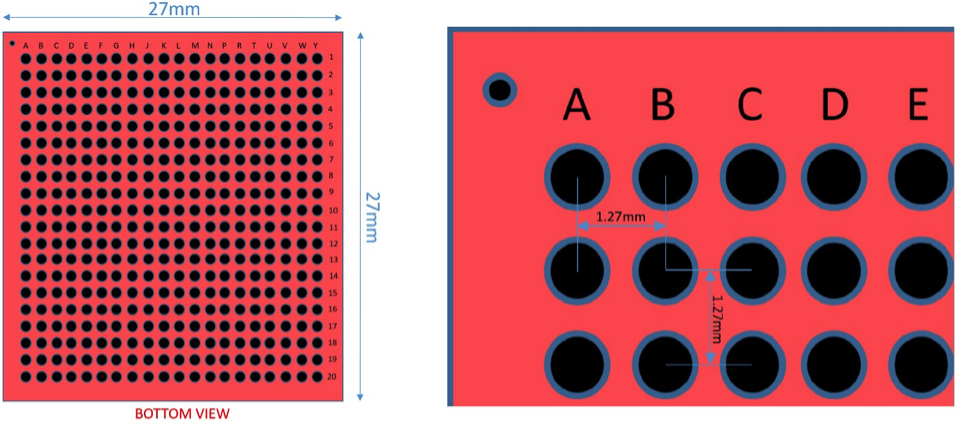
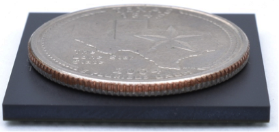
The OSD335x C-SiP comes in a 27mm x 27mm Ball Grid Array (BGA) package with 400 balls and 1.27mm ball pitch as shown in Figure 2. The diameter of the balls is 0.5mm and edge to edge spacing is 0.77mm.
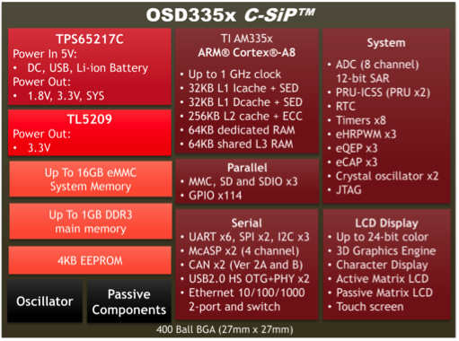
OSD335x C-SiP consists of seven main components as shown in Figure 3. They are:
- Sitara® AM335x ARM® Cortex® A8 processor from TI.
- TPS65217 Power Management IC (PMIC) from TI – manages power distribution to various components within the SiP and provides power to external devices.
- TL5209 Low Drop Out (LDO) regulator from TI – provides a dedicated 3.3V rail to power components external to the SiP.
- Up to 1GB of DDR3 – is the main memory.
- Up to 16GB of eMMC Non-Volatile memory – stores the operating system as well as other files and other software applications.
- 4KB EEPROM – stores important hardware and configuration information.
- MEMS Oscillator – primary clock for the AM335x processor.
All of the peripheral interfaces of the AM335x (except the DDR and eMMC interface) are brought out to pins on the OSD335x C-SiP. See the OSD335x C-SiP datasheet for more information on the pinout.
Reference Design Lesson Organization
This document heavily relies on OSD335x Tutorial Series Reference Design Lessons 1 and 2. Each section will review the highlights of each tutorial article as well as any special consideration needed for the OSD335x C-SiP implementation. It is helpful to understand how Lesson 1 and Lesson 2 are organized before proceeding with this document.
Lesson 1 and Lesson 2 begin with an Introduction section, which describes the objective of the lesson, followed by a series of articles, each of which will walk you through the design methodology. The lessons each conclude with an Expected outcome section, which describes how the outcome of that lesson will look.
Furthermore, the Lessons will have several Perks and Caveats. The Perks will give additional information about the topic in discussion and the Caveats will warn you about conditions or situations which require more attention. The Perks and Caveats look like this:


Before proceeding with this document, we strongly encourage you to read the OSD335x C-SiP datasheet.
Pre-requisites
Both Lesson 1 and Lesson 2 use Autodesk Eagle for schematics and layout. Hence, we assume that you are familiar with Eagle schematics and layout. If not, please learn about them first. The following website is one of the many websites that can help you:
To learn more about schematics: https://learn.sparkfun.com/tutorials/using-eagle-schematic
To learn more about layout: https://learn.sparkfun.com/tutorials/using-eagle-board-layout
Introduction to Bare Minimum Circuitry to Boot OSD335x C-SiP
The objective of this section is to help you become familiar with the bare minimum setup required to boot the OSD335x C-SiP and getting it ready to execute software. This section will walk you through every step of OSD335x Reference Design Lesson 1.
Please read Introduction to Bare Minimum Circuitry to Boot OSD335x article to understand the CAD setup required to put together bare minimum circuitry. While setting up the CAD environment, please keep in mind that the OSD335x C-SiP comes in a 27mm x 27mm package with an updated ball map as shown in Figure 4.
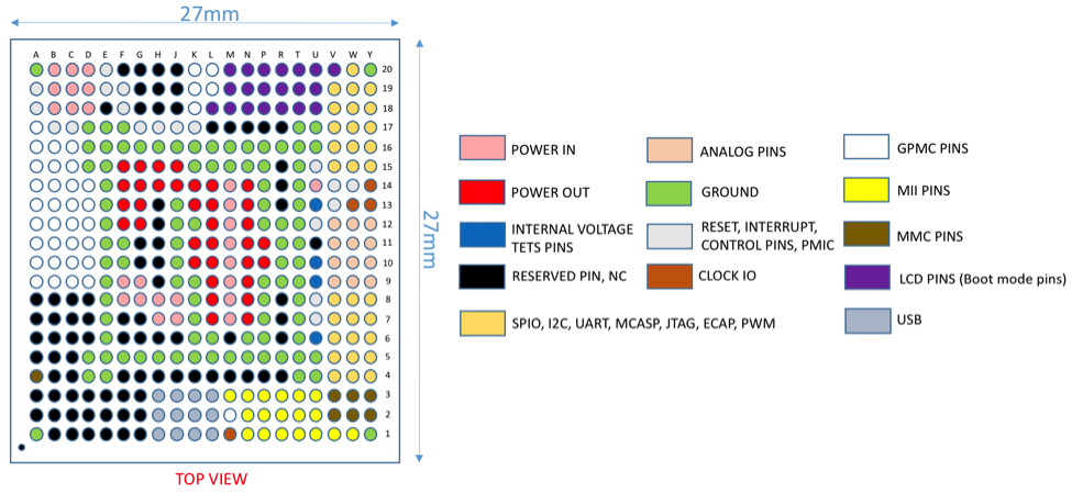
The OSD335x C-SiP ball map has been optimized to help you bring out all the signals on a single layer of PCB. OSD335x C-SiP Layout Guide talks about good layout practices recommended for OSD335x C-SiP and also provides several layout examples.
OSD335x C-SiP Power Inputs and Outputs
OSD335x-SM Power Circuitry is very similar to that of OSD335x-BAS. Hence, to find detailed information on how to configure Power I/O for OSD335x family of devices, please refer to the OSD335x Power Inputs and Outputs article of OSD335x Reference Design Lesson 1.
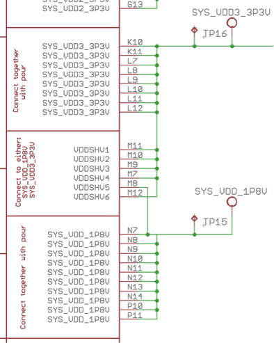
VDDSHVx Pins on the OSD335x C-SiP
Unlike OSD335x, the VDDSHVx pins are externally accessible on the OSD335x C-SiP. Hence, the I/O domain voltages are not fixed to 3.3V on the OSD335x C-SiP. Each domain is user adjustable to either 1.8V or 3.3V. The VDDSHVx pins of the OSD335x C-SiP (i.e., VDDSHV1 thru VDDSHV6) must be connected to either a 1.8V or 3.3V power source to provide required voltage to the I/O power domains.
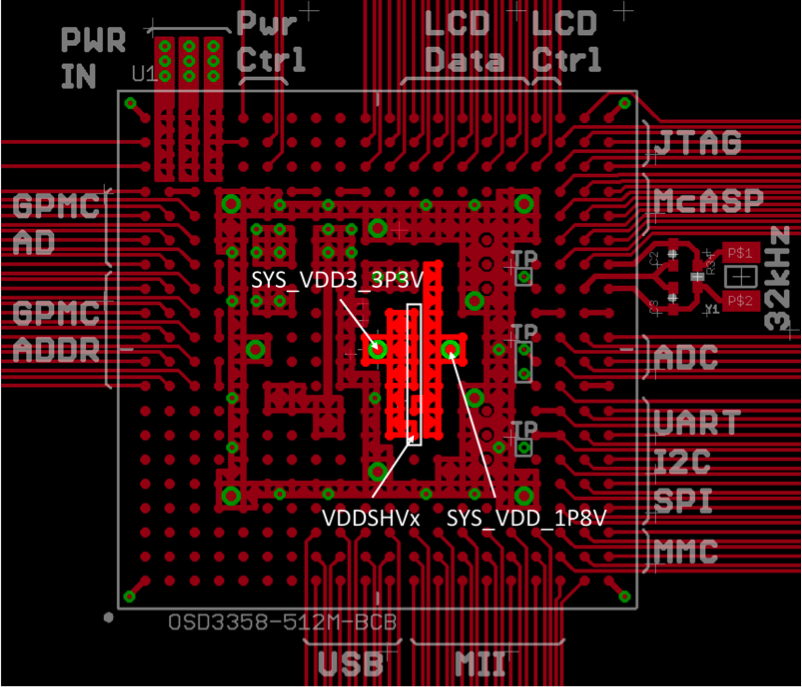
Figure 5 and Figure 6 show example schematic and layout snippets where VDDSHV5 ball is connected to SYS_VDD_1P8V balls and the rest of VDDSHVx balls are connected to SYS_VDD3_3P3V balls.
To find out what IOs each of these IO domains correspond to, please refer to the AM335x datasheet.
SYS_VDD3_3P3V on the OSD335x C-SiP
The OSD335x C-SiP provides an additional 3.3V output power rail, SYS_VDD3_3P3V, which can be used to power the I/O domains (VDDSHVx pins) as shown in Figure 5. This power rail is supplied by LDO4 of TPS65217 PMIC.
VREFN on the OSD335x C-SiP
The OSD335x C-SiP also features an Analog Negative Reference Input (VREFN) which was not externally accessible on the OSD335x. The 12bit ADC on the OSD335x C-SiP has a maximum voltage range of 0 to 1.8V. If you want to use the full voltage range, connect VREFP to 1.8V and VREFN to AGND. However, if your application needs a narrower voltage range for higher precision, you can achieve this by connecting VREFP and VREFN appropriately.
VDDS and VDDS_RTC Pins on the OSD335x C-SiP
VDDS is the power input for AM335x 1.8V IO domain and VDDS_RTC is the power input for the AM335x RTC power domain. These pins are brought out to pins on the OSD335x C-SiP, whereas, they were internally connected to the PMIC on the OSD335x.
VDDS must be powered by a 1.8V power rail. It should be connected to the SYS_RTC_1P8V rail.
VDDS_RTC connection depends on the state of RTC. VDDS_RTC input power rail should also be powered by SYS_RTC_1P8V when RTC needs to be enabled. But, VDDS_RTC should be connected to RTC_KALDO_ENN when RTC is disabled. See the Minimum Processor PMIC interface Connections and Minimum RTC Power Connections sections of OSD335x C-SiP datasheet to learn more about other connections necessary to enable or disable the RTC.
The ball M13 is close to the SYS_RTC_1P8V balls (K13, K14, L13, L14) to make power routing easy. Similarly, ball U14 is close to RTC_KALDO_ENN (U15) so that these two pins can be easily connected together when RTC is disabled. It is not necessary to connect both M13 and U14 since the power draw of VDDS_RTC is very small.
EMMC_VCC and EMMC_VCCQ
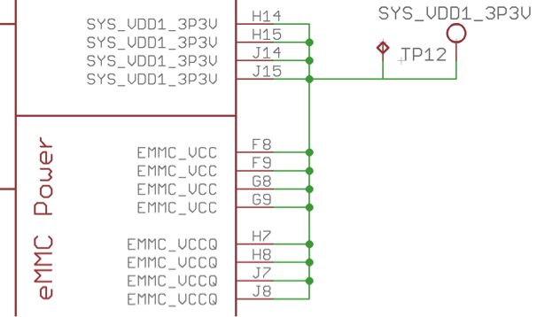
EMMC_VCC and EMCC_VCCQ are the 3.3V power inputs for the core and I/O of eMMC present inside the OSD335x C-SiP respectively. These eMMC power inputs should be powered using the SYS_VDD1_3P3V output power rail as shown in Figure 7. However, it is possible to use external 3.3V power rails to power the eMMC, if necessary for a given application.
OSD335x C-SiP Ground Connections
The OSD335x Ground Connections article of Reference Design Lesson 1 has good recommendations for setting up proper ground planes and the theory behind grounding.
For specifics on grounding the OSD335x C-SiP please refer to the OSD335x C-SiP Layout Guide.
OSD335x C-SiP Power Management
The Power Management article of Reference Design Lesson 1 will help you configure the Power Management Circuitry of OSD335x C-SiP. Adding on to the features of OSD335x, OSD335x C-SiP makes power management easier by providing:
- PMIC Reset control through PMIC_NRESET pin
- Internal LDO (TL5209) control through SYS_VDD1_CTL pin
- PMIC internal MUX control through PMIC_MUX_IN and PMIC_MUX_OUT pins
Each of the above features are discussed below.
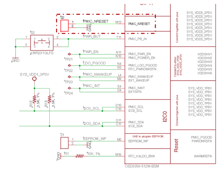
PMIC_NRESET pin
In addition to the features mentioned in Power Management article, the OSD335x C-SiP features a PMIC_NRESET pin which can be used to reset the TPS65217C Power Management IC (PMIC). Generally, it is recommended to add a jumper or test pad to your design to provide the ability to pull this pin low. An example where PMIC_NRESET is connected to a ground jumper is shown in Figure 8.
SYS_VDD1_CTL Pin
SYS_VDD1_CTL is the active high enable pin for the TL5209 LDO inside the OSD335x C-SiP. This pin is internally pulled up on the OSD335x C-SiP. Hence, TL5209 (SYS_VDD1_3P3V) will remain active when this pin is left unconnected. Connect this pin to ground to disable the TL5209 internal LDO and thereby turn off the SYS_VDD1_3P3V output power rail if not needed.
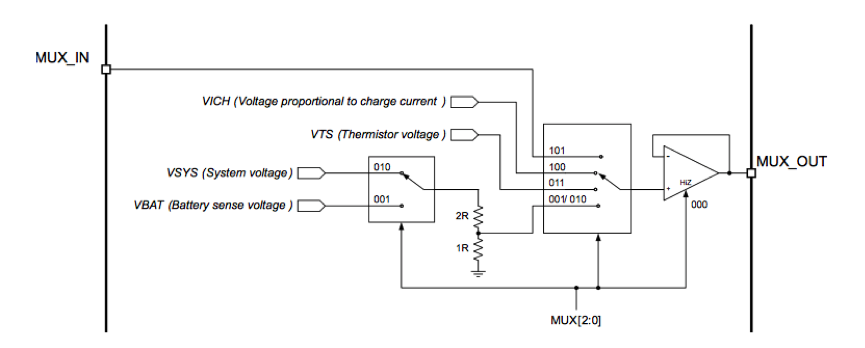
PMIC_MUX_IN and MIC_MUX_OUT Pins
The OSD335x C-SiP also brings out PMIC_MUX_IN and PMIC_MUX_OUT pins from the TPS65217C PMIC. Using PMIC_MUX_OUT, critical system voltages of PMIC such as VBAT, VSYS, VTS and VICH can be accessed. One additional external input, i.e., PMIC_MUX_IN is available to monitor an additional system voltage. Feature Description diagram of PMIC Analog Multiplexer is shown in Figure 9. For more information on Analog Multiplexer, refer Analog Multiplexer section of TPS65217 datasheet.
OSD335x C-SiP Clamping Circuit
The AM335x datasheet requires that the voltage difference between the power rails VDDS (i.e., SYS_RTC_1P8V power input of OSD335x C-SiP) and VDDSHVx [1-6] (when connected to 3.3V source) of the AM335x processor be less than 2V during the entire power-down sequence. More information about this can be found under Use of a Clamping Circuit for Simultaneous Ramp Down section of this user guide.
Your design may or may not need a clamping circuit based on the above requirement.
If you think your design needs a clamping circuit, please refer the Clamping Circuit article of OSD335x Reference Design Lesson 1 to find out more information.
OSD335x C-SiP ESD Protection
ESD Protection is essential for every electronic design. OSD335x ESD Protection article of Reference Design Lesson 1 will give you good recommendations on ESD.
OSD335x C-SiP Reset Circuitry
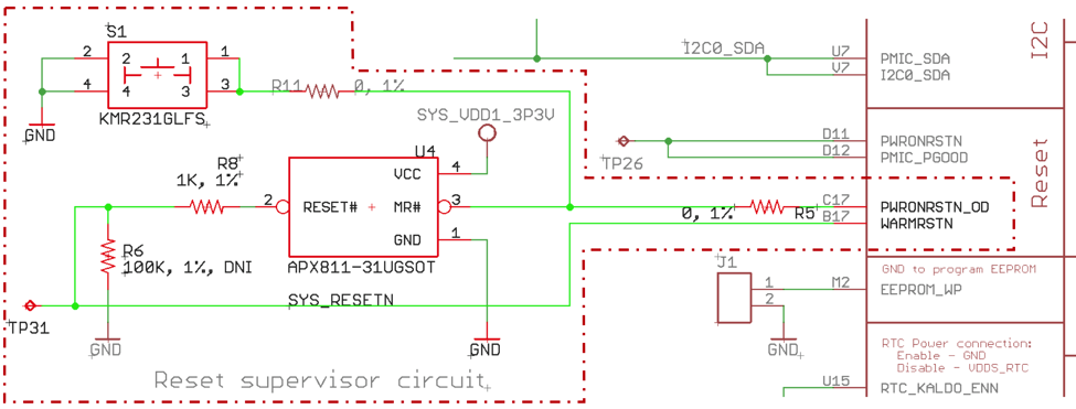
Please read the OSD335x Reset circuitry article to understand how to configure reset circuitry for OSD335x. One important difference to note in the case of OSD335x C-SiP is that it has an integrated open drain buffer (SN74LVC1G07) internally connected to PWRONRSTN. The output of this buffer is brought out as PWRONRSTN_OD pin. Hence, an external open drain buffer is not necessary between PWRONRSTN and WARMRSTN as described in OSD335x Reset circuitry article in the case of the OSD335x C-SiP.
A supervisor circuit and a manual reset button can be connected between PWRONRSTN_OD pin and WARMRSTN pin as shown in Figure 10.
OSD335x C-SiP Clock Circuitry
The OSD335x C-SiP integrates a low power, low jitter MEMS Oscillator that provides the main input clock to the AM335x on OSC0. The MEMS Oscillator is the primary clock source for the AM335x. The active high enable input for the MEMS Oscillator is brought out as OSC0_CTL pin on the OSD335x C-SiP. This pin has an internal pull up resistor in the SiP so it can be externally connected to a test point. This allows the processor clock to be disabled if necessary. To know more about the parameters of MEMS Oscillator, refer MEMS Oscillator section of OSD335x C-SiP datasheet.
Please use the OSD335x Clock Circuitry article to understand how to build the clock circuitry for RTC clock input (OSC1) of the OSD335x C-SiP.
OSD335x C-SiP Peripheral Circuitry
To know how to connect basic peripherals and also understand how to setup boot configuration, please read Peripheral Circuitry article of OSD335x Lesson 1. Keep in mind that on the OSD335x C-SiP, the boot mode resistors (SYSBOOT[15:14]) have already been set appropriately to match the MEMS oscillator frequency within the device (i.e. a value of 0b01to signify a 24 MHz input).
OSD335x C-SiP Bare Minimum Boot process
To understand the process of loading and running a bare metal application on OSD335x C-SiP, please go through the OSD335x Bare Minimum Board Boot Process article of Reference Design Lesson 1.
Introduction to Bare Minimum Circuitry for Linux Boot
The objective of this section is to help you become familiar with the bare minimum setup required to boot Linux on the OSD335x C-SiP by building upon concepts and PCB design that were presented as part of OSD335x Reference Design Lesson 1.
Lesson 2 (section 12 to section 18) of this article enables you to build a new PCB by appending additional features recommended for booting Linux to the Lesson 1 PCB design.
Please read Introduction to Bare Minimum Circuitry to Linux Boot article to understand the CAD setup required to put together bare minimum circuitry. While setting up the CAD environment, please keep in mind that the OSD335x C-SiP comes in a 27mm x 27mm package with an updated ball map.
USB Circuitry
The USB Circuitry article will give you necessary information about the different USB pins, how to put the USB peripherals of the OSD335x C-SiP into the different USB modes, schematic/layout methodology and USB Testing for the OSD335x C-SiP.
Adding Non-Volatile Storage
The Adding Non-Volatile Storage article will help you connect a SD card to the OSD335x C-SiP by giving you necessary information about their corresponding circuits, schematic and layout. Since the eMMC and EEPROM are already incorporated into the OSD335x C-SiP device, you can disregard the instructions for adding eMMC and EEPROM in the Adding Non-Volatile Storage article.
However, there are few things that need to be kept in mind:
- The eMMC interface pins of the AM335x (GPMC_AD0 to GPMC_AD7, GPMC_CSN1 and GPMC_CSN2) are not externally accessible.
- The active low eMMC reset pin is externally available on the OSD335x C-SiP as the EMMC_RSTN pin. This pin has an internal pull up resistor and hence can be left floating if unused.
- The Write Protect pin for the EEPROM is brought out of the OSD335x C-SiP as EEPROM_WP pin. It is recommended that this pin be connected to a test point or a ground jumper in your design so that it can be grounded whenever the EEPROM needs to programmed.
Additionally, since the OSD335x-C-SiP supports both 3.3V and 1.8V IO, the following caveat should be used instead of the one in the OSD335x section
Bringing Up a Custom Bare-Bones Linux PCB
The Bringing Up a Custom Bare-Bones Linux PCB article will help you will finalize the Lesson 2 board design and bring up the manufactured printed circuit board (PCB). After bringing up the board, you can explore new applications with your completed design and use the design as a starting point for future application specific designs.
Linux Boot Process with the OSD335x
The Linux Boot Process with the OSD335x article focuses on understanding the boot process of a OSD3358-SM-RED Debian Linux image running on OSD335x C-SiP. The article will walk you through the functions of different software layers that are responsible for Linux boot on OSD335x C-SiP such as the ROM bootloader, SPL and U-Boot.
Linux Device Tree
The Linux Device Tree article will help you get started with Linux device trees by introducing the structure of device trees, describing some properties of device trees and showing you how to modify an existing device tree for your custom hardware configuration
Linux Device Tree Overlay
The Linux Device Tree Overlay article will help you become familiar with device tree overlays by explaining the structure through an example, building a device tree overlay for the peripheral header of the Lesson 2 board, and then adapting the generic overlay for an example MikroElektronika mikroBUS™ click board™
*****
