OSD335x Lesson 2: Introduction to Bare Minimum Circuitry for Linux Boot
Published On: April, 20, 2018 By: Eshtaartha Basu | Updated: August 27, 2018 by Eshtaartha Basu
1 Introduction to Bare Minimum Circuitry for Linux Boot
1.1 Introduction
The objective of this lesson is to help you become familiar with the bare minimum setup required to boot Linux on the OSD335x by building upon concepts and PCB design that was presented as part of Lesson 1. Similar to Lesson 1, this lesson will consist of a series of articles which will walk you through every step of the design process. We start from specifications and guide you through every step till debugging the manufactured Printed Circuit Board (PCB). The lesson will conclude with a PCB that verifies the design by putting together everything that was taught.
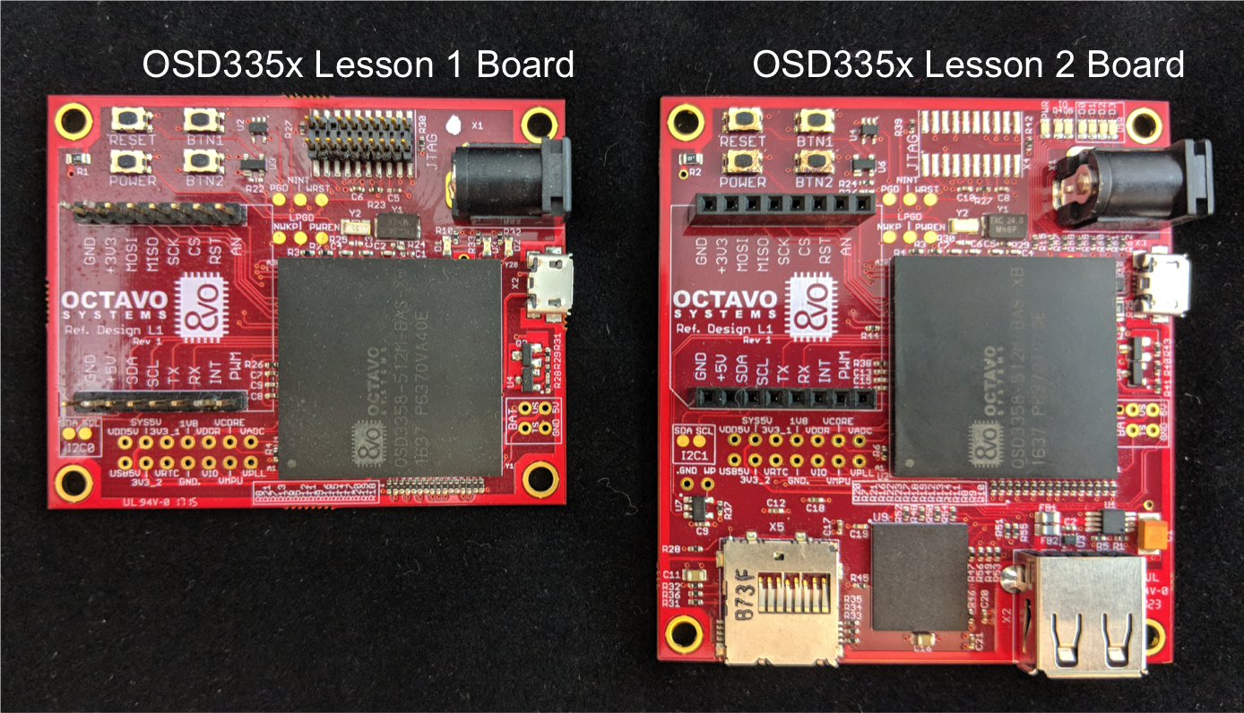
Recall that in Lesson 1, we built a PCB that could boot a bare metal application (using TI Starterware) on OSD335x without the need of an OS. In Lesson 2, we will be adding USB connectivity and non-volatile memory to the Lesson 1 PCB design so that it can boot Linux. Lesson 1 PCB and expected Lesson 2 PCB designs that you can build yourself by following the steps.
Similar to Lesson 1, this lesson will consist of a series of articles which will walk you through every step of the design process. We start from specifications and guide you through every step till debugging the manufactured Printed Circuit Board (PCB). The lesson will conclude with a PCB that verifies the design by putting together everything that was taught.
Table of Contents
1Introduction to Minimal Linux Boot
1.1Introduction
1.2CAD Environment Setup
1.2.1Library Setup
1.2.2Schematic Setup
1.2.3.Layout (Board) Setup
1.3OSD3358-512M-BAS Pin Distribution
![]()
![]() A PDF version of this Lesson as well as the entire OSD335x Design Tutorial can be downloaded here.
A PDF version of this Lesson as well as the entire OSD335x Design Tutorial can be downloaded here.

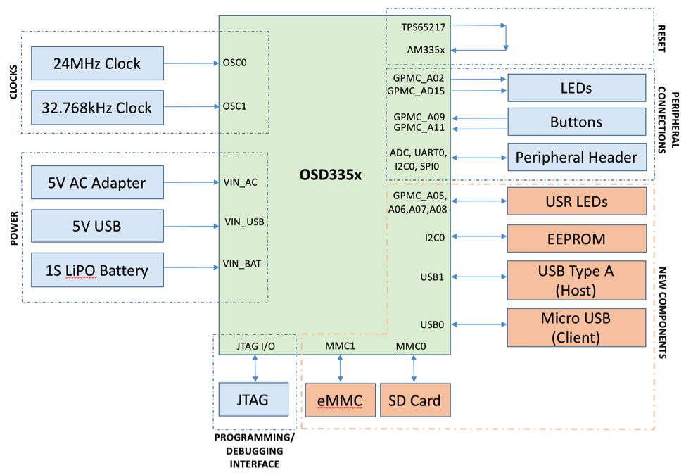
For Lesson 2, we will be starting from the Lesson 1 block diagram and adding connectivity and non-volatile storage in order to demonstrate some of the capabilities of Linux as shown in Figure 1. We will walk through articles on:
- USB circuitry which will provide connectivity
- MMC circuitry which will provide non-volatile storage
- EEPROM circuitry which will provide non-volatile board configuration information
- Useful information on configuring the Linux Device Tree for a new board
- Tips on board bring-up and debug as well as demo examples
1.2 CAD Environment Setup
The Lesson 1 PCB design will serve as a foundation for Lesson 2. Hence, we need to first download and open Lesson 1 Eagle PCB Design files. You can download Lesson 1 design files here.
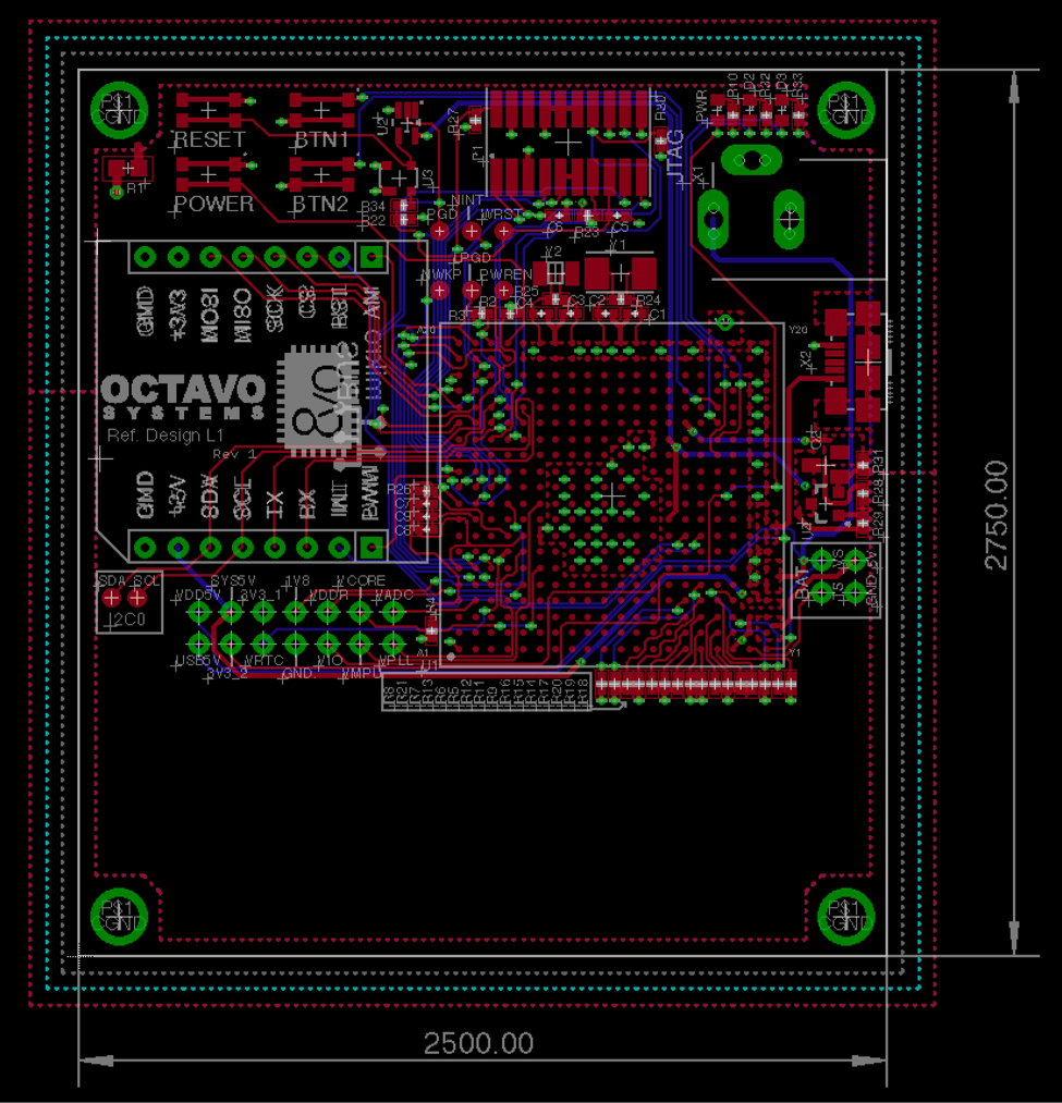
To accommodate the additional components, we will need to increase the length of Lesson 1 PCB. Except the length all other parameters can be maintained the same:
- New Board Size: 2500mil x 2750mil (2.5inch x 2.75inch)
- Number of layers: 4 layers
- Trace width: 6mil (approx. 0.15mm). Since power traces generally carry more current, we will be using larger traces (at least 15mil or 0.4mm) for them. o Trace spacing: 6mil (approx. 0.15mm)
- Trace spacing: 6mil (approx. 0.15mm)
- Minimum drill and via size: 12mil (approx. 0.30mm) drill and 24mil (approx. 0.60mm) finished via diameter (i.e., 6 mil annular ring)
Using these standard PCB design rules will help us reduce manufacturing cost. For your design, you are free to select the appropriate rules for your manufacturer and components that suit your design.
1.2.1 Library Setup
Octavo Systems provides an updated Eagle library for Lesson 2, OSD3358_BAS_RefDesignParts_L2.lbr, that contains the schematic symbol and footprint for all the additional components required for Lesson 2. The library can be downloaded here.
1.2.2 Schematic Setup
- Rename the Lesson 1 schematic file RefDesL1.sch as RefDesL2.sch and layout file RefDesL1.brd as RefDesL2.brd.
- Make sure Eagle is setup properly to use the updated Lesson 2 library (OSD3358_BAS_RefDesignParts_L2.lbr).
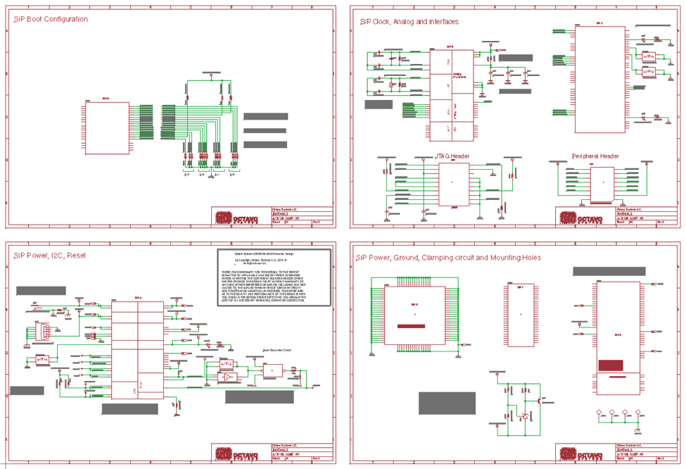
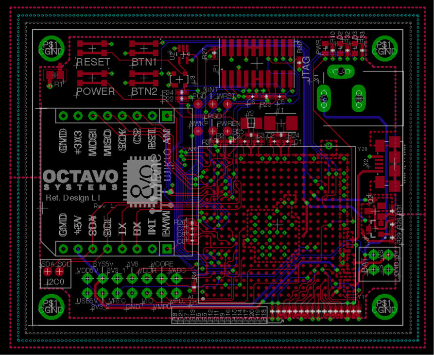
- OpenRefDesL2.sch. The schematic should look similar to Figure 2. This will serve as a good starting point for Lesson 2 design.
- It is up to you to change the label, date and revision number on each schematic page as necessary.
1.2.3 Layout (Board) Setup
- Open RefDesL2.brd file.
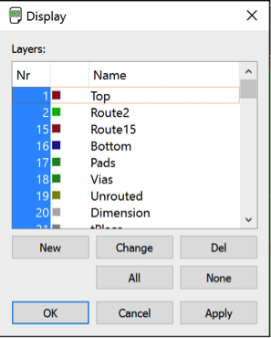
- The layer stack up is shown in Figure 3. We’ll be using Top and Bottom layers for signal routing. Route2 layer acts as power plane. Route15 layer acts as ground plane.
- The layout should look similar to Figure 4.
- Extend the lower end of the PCB boundary and move the ESD rings by 750mils to make space for new components that will be added in this lesson. After the extension, the layout should look similar to Figure 5.
1.3 OSD3358-512M-BAS Pin Distribution
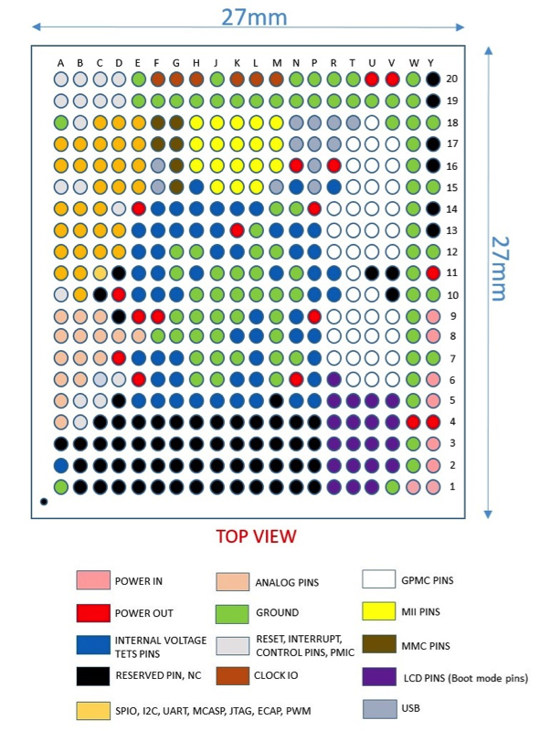
Figure 6 gives visual representation of the OSD335x BGA pin arrangement. This will help us plan the placement of additional components on Lesson 2 board.
*****
| << Return to “OSD335x Lesson 1 Bare Minimum Board Boot Process” | Continue to “OSD335x Lesson 2 USB Circuitry” >> |
