OSD335x Ground Connections
Published On: August, 1, 2017 By: Eshtaartha Basu | Updated: July 18, 2018 by Cathleen Wicks
Introduction
This article is the second part of the OSD335x Reference Design Lesson 1 Power circuitry article. It will focus on ground connections and pours required for reliable performance from the OSD335x. As we discuss the power circuitry, we will build the schematic and layout the corresponding traces.
Prerequisite
This article is a part of the broader OSD335x Reference Design Lesson 1 series which consists of a sequence of articles designed to help you build the bare minimum circuitry required to boot the OSD335x.
We recommend reading the first part of power circuitry article OSD335x Power Inputs and Outputs before this one. This article builds upon the foundation outlined in it.
All design files for this lesson can be downloaded here.
This articles as well as the entire OSD335x Design Tutorial can be downloaded here.
Ground Connections
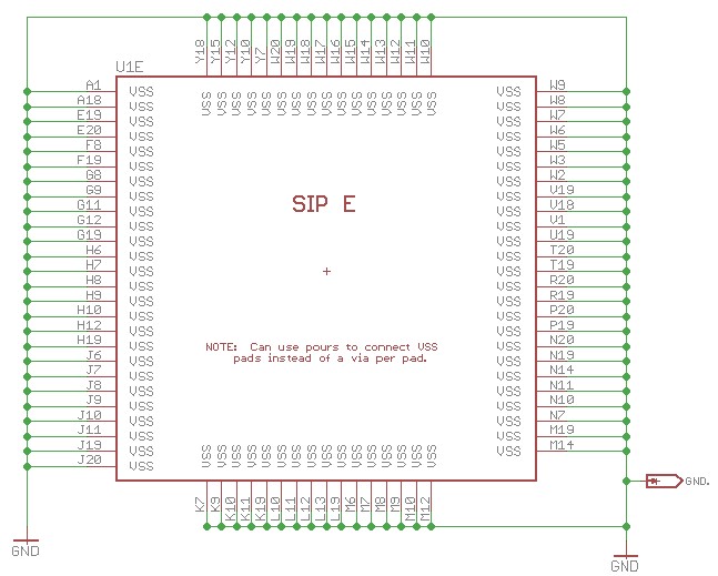
The OSD335x has several ground pins. All the pins on the SIP E symbol should be grounded, as shown above in Figure 1, even though they are connected together within the SiP. This is to make sure all components within the OSD335x are uniformly grounded and ensure the shortest return current paths for all the components inside the OSD335x. For our reference design, a thru-hole test point was added to help us measure voltage during bring-up.
It is good to have test points to ground on the design for testing during bring-up. But, it is not necessary as long as there is access to ground somewhere in the design. In compact designs, you can use surface test points to save space.
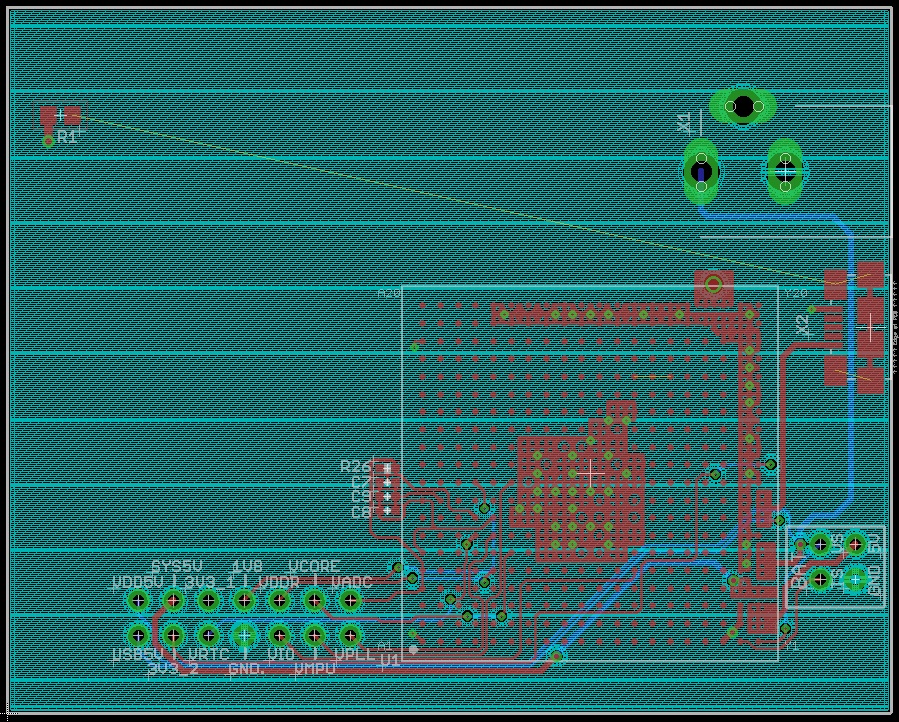
Ground pour layout discussion
When grounding the OSD335x, you are free to use one via for each ground pin. However, vias occupy a lot of routable space and a lot of vias can cause routing problems (this does not necessarily apply to blind and buried vias since they occupy much less route-able board area). Routable space can be saved by instead using ground pours and minimizing the number of ground vias. For this design, since the ground pins are clustered in two areas, we have placed two copper pours on the top layer for ground. Then we have at least one via per two ground pins so there is a good connection to the ground plane. When using copper pours, the following things should be considered:
- Have at least one via for every two to four ground pins.
- Vias should be placed wisely keeping current return path also in mind.
- Care should be taken not to flood the entire area below the BGA of the OSD335x with a ground pour. If the area of the ground pour is large, it may sink too much heat from the BGA and may result in bad solder joints during reflow. Similarly, make sure thermals are used for the pours to prevent the pours from sinking too much heat and causing bad solder joints.

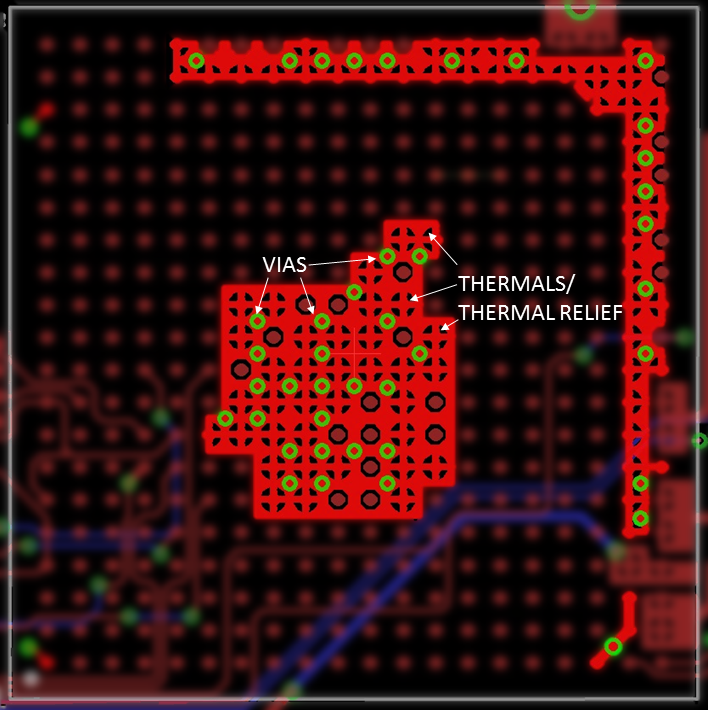
As shown in Figure 2, we have used two ground pours for this design to minimize the size of each pour. Each pour uses and there are plenty of vias to ensure good connection to ground.
Power and Ground Planes
As we already stated, our design uses a 4 layer PCB. The top and the bottom layers are used for signal routing. The layer beneath the top layer is used as a power plane. The layer below the power plane is used as a ground plane. Use of power and ground planes that are closely spaced to each other reduces cross-talk. It also reduces interference between the top and bottom signal layers.
Most of the components in this design will operate on 3.3V. Hence, we will be connecting SYS_VDD_3P3V to the power plane. The power plane will help those components directly receive power through a via with minimal resistance since the power plane is spread across the board.
The ground plane is used to connect all components to a common ground reference. It will:
- provide a low resistance return path for currents to reduce noise.
- will prevent current loops.
- will act as EMI shield protecting the PCB from external noise. It will also prevent radiation of high frequency noise from the PCB.
- provide uniform impedance plane for traces carrying high frequency signals with high fidelity against reflections.
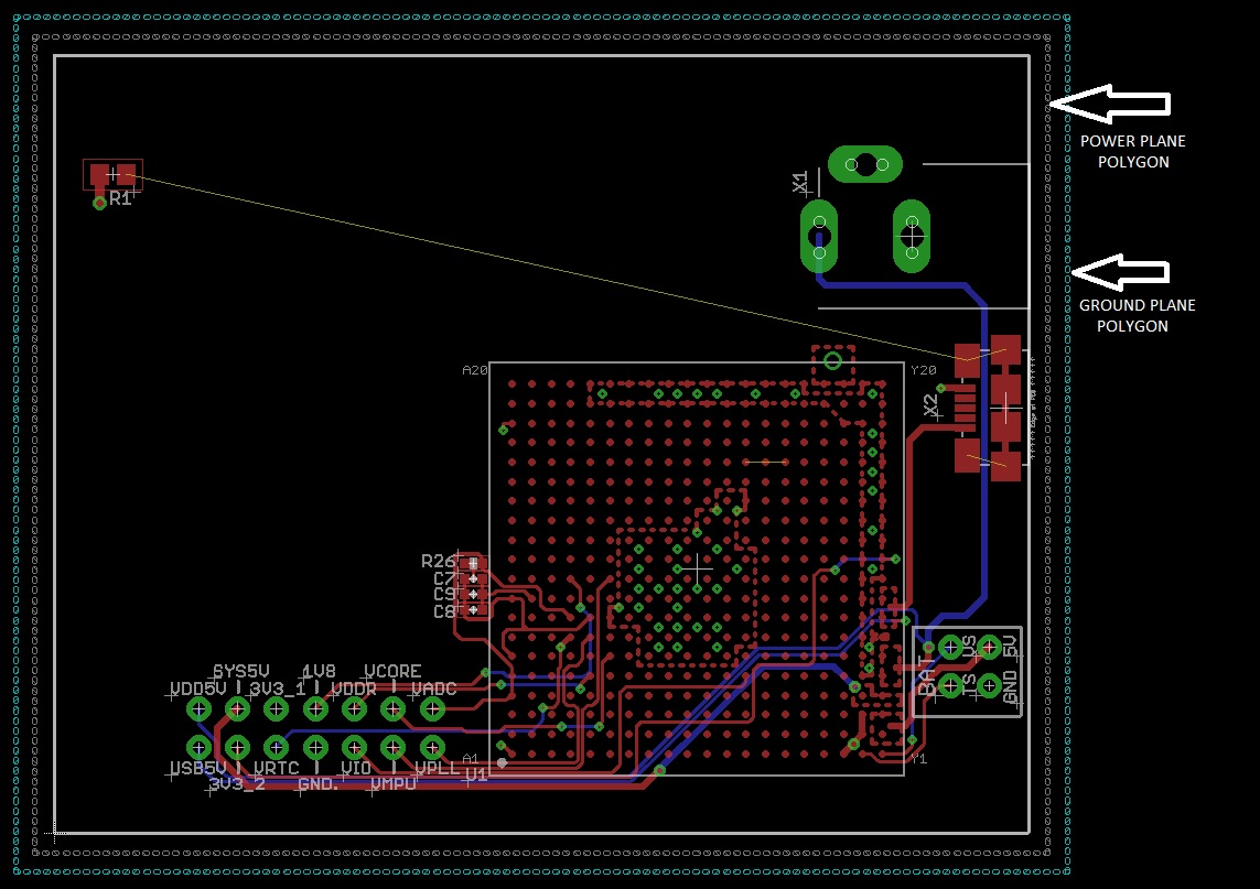
Power and Ground planes can be created in the layout by drawing one complete polygon along the edge of the board in layer 2 and connecting it to SYS_VDD_3P3V and drawing the other complete polygon in Layer 15 and connecting it to GND using the NAME tool of Eagle. The POWER and GND polygons are shown in Figure 3.
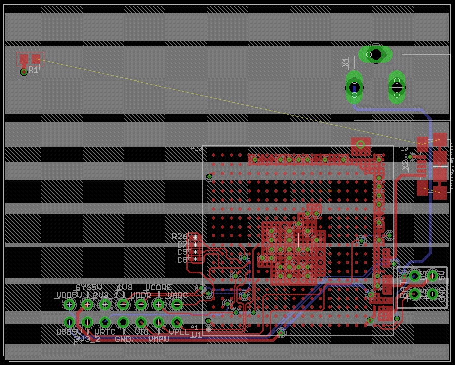
When the RATSNEST button is pressed on the layout, the power and ground planes occupy the entire area of the board as shown in Figure 4 and Figure 5.
| << Return to “OSD335x Power Inputs and Outputs” | Continue to “OSD335x Power Management” >> |
