OSD335x ESD Protection
Published On: August, 1, 2017 By: Eshtaartha Basu | Updated: July 18, 2018 by Cathleen Wicks
Introduction
Electrostatic discharge (ESD) is the flow of a static electric charge from one object to another when two charged objects come into contact. Familiar examples of ESD include the shock we receive when we walk across a carpet and touch a metal door knob and the static electricity we feel after drying clothes in a clothes dryer. This flow of static charge involves build-up of a very high voltage (around 10KV) for a very short duration of time. Generally, a Printed Circuit Board (PCB) receives an ESD strike whenever a person (whose skin is statically charged) touches it. Most electronic components (without internal ESD protection) get damaged since they cannot withstand such high voltage. Hence, ESD protection for a PCB is essential to protect all the components on it.
Prerequisite
This article is a part of the broader OSD335x Reference Design Lesson 1 series which consists of a sequence of articles designed to help you build the bare minimum circuitry required to boot the OSD335x.
We recommend reading the fourth part of power circuitry article OSD335x Clamping Circuit before this one. This article builds upon the foundation outlined in it.
All design files for this lesson can be downloaded here.
This articles as well as the entire OSD335x Design Tutorial can be downloaded here.
ESD protection
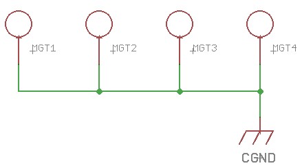
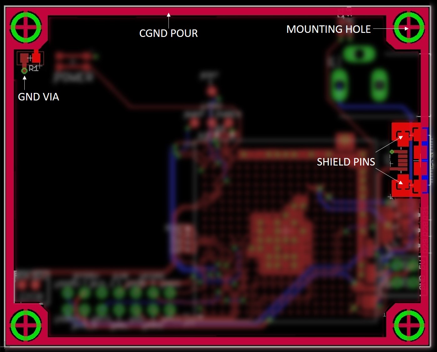
In order to protect the board from ESD strikes which can result from a person touching the PCB, we have created a ground ring, CGND, that runs along the edge of the PCB on both the top and bottom layers. The ground ring connects all of the mounting holes (annotated in Figure 4) and shield pins (annotated in Figure 4) of metal connectors, such as USB connectors. These components are most susceptible to ESD strikes. An ESD strike has a very high voltage (around 10KV), but relatively little charge (low energy). Therefore, we can use a couple of different methods to help dissipate the energy from an ESD strike.
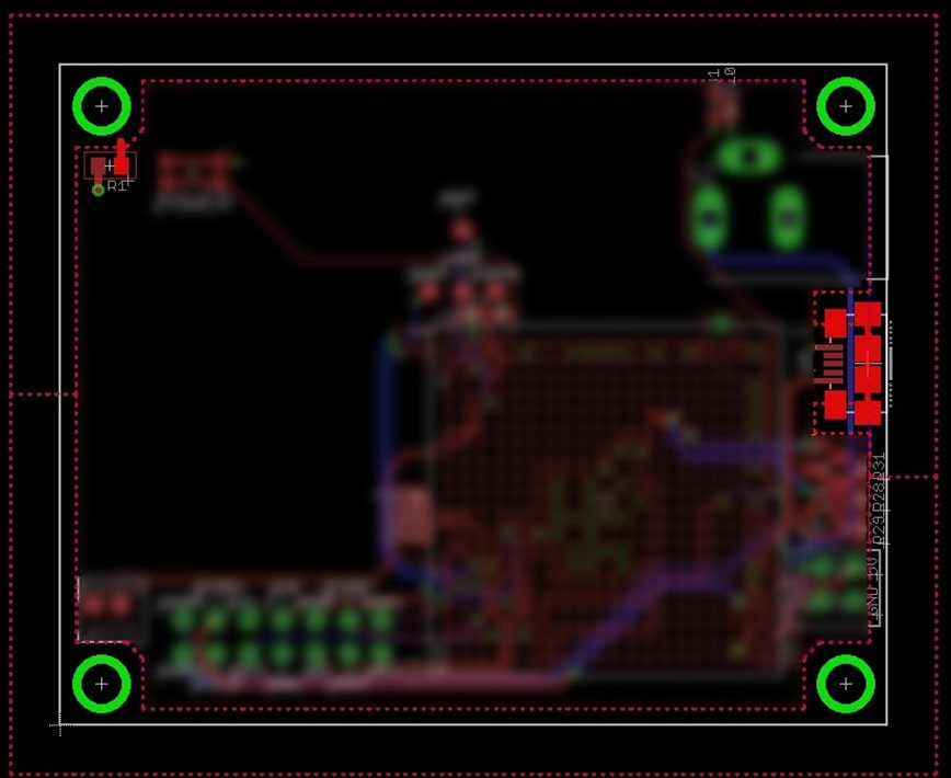
First, we can make use of the mounting holes as shown in Figure 1. Four mounting holes are placed at the corners of the PCB for mechanical attachments to the board. Generally, PCBs are bolted through the mounting holes to metal cases that are externally grounded. As a result, when an ESD strike occurs, the charge safely flows through the mounting holes to the bolts and finally to external ground.
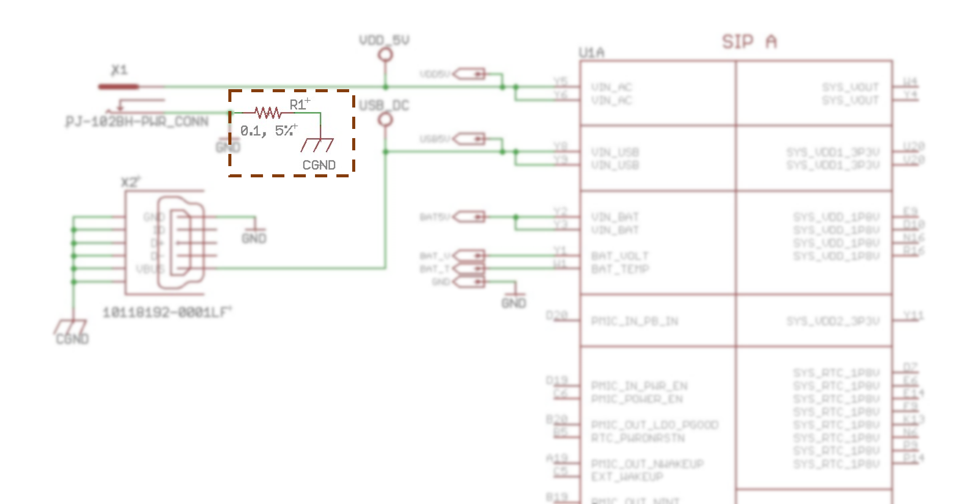
Second, since a PCB may not be mounted and not have a path to external ground, we can add circuitry to dissipate the energy through the ground (GND) plane. Therefore, CGND is connected to the GND plane of the PCB through a 0.1 ohm resistor (R1) as shown in Figure 2 (This picture is from OSD335x Power Inputs and Outputs).
This will make sure any ESD strike can be safely dissipated into the GND plane. The 0.1 ohm resistor should have a higher wattage (0.125W or larger) to make sure there are no thermal issues (damage to the resistor due to power flow that exceeds its rating). Alternately, a 0.1uF capacitor and 100K Ohm resistor in parallel can be used to connect CGND to the GND plane (In this design, we have opted for the single resistor approach to dissipate energy since it is more economical).
The CGND polygon pour for ESD protection should form a complete ring along the edge of the board and must be well connected to the shield pins of the connectors. The CGND polygon pour must be present on both sides of the board. For this design, we will use a pour of at least 50 mils as shown in Figure 3 and Figure 4.
| << Return to “OSD335x Clamping Circuit” | Continue to “OSD335x Reset Circuitry” >> |
