OSD335x-SM Layout Guide
Published On: September, 17, 2017 By: Eshtaartha Basu | Updated: July 18, 2018 by Cathleen Wicks
Introduction
The OSD335x-SM was designed to minimize the number of Printed Circuit Board (PCB) layers and make the layout process easy. This document will cover important aspects of PCB layout design specific to the OSD335x-SM and help designers quickly begin the PCB layout process. First, this document will discuss the layout of the OSD335x-SM BGA. Then it will discuss a few common layout scenarios using relevant examples with recommendations on pours for Power, Ground, IO domains, Clamping Circuit and other supporting circuitry.
This document assumes that the reader is already familiar with layout design process and the OSD335x-SM (OSD335x-SM Data Sheet). It should not be used as a comprehensive layout tutorial or a generic layout design guide.
![]()
![]() A PDF version of this App Note can be found here.
A PDF version of this App Note can be found here.

1. OSD335x-SM Layout Specifications
The OSD335x-SM Family of System-In-Package (SiP) products are building blocks designed to allow easy and cost-effective implementation of systems based on Texas Instruments’ powerful Sitara™ AM335x line of processors. The OSD335x-SM integrates the AM335x along with the TI TPS65217C PMIC, the TI TL5209 LDO, up to 1 Gigabyte (GB) of DDR3 Memory, a 4 Kilobyte (KB) EEPROM for non-volatile configuration storage and resistors, capacitors, and inductors into a single 21mm x 21mm design-in-ready package.
This section will introduce important specifications, ball mapping and footprint information of the OSD335x-SM.
1.1 Background Information
To understand layout guidelines and methodology used for the recommendations made in this document in more detail, please refer to the following documents:
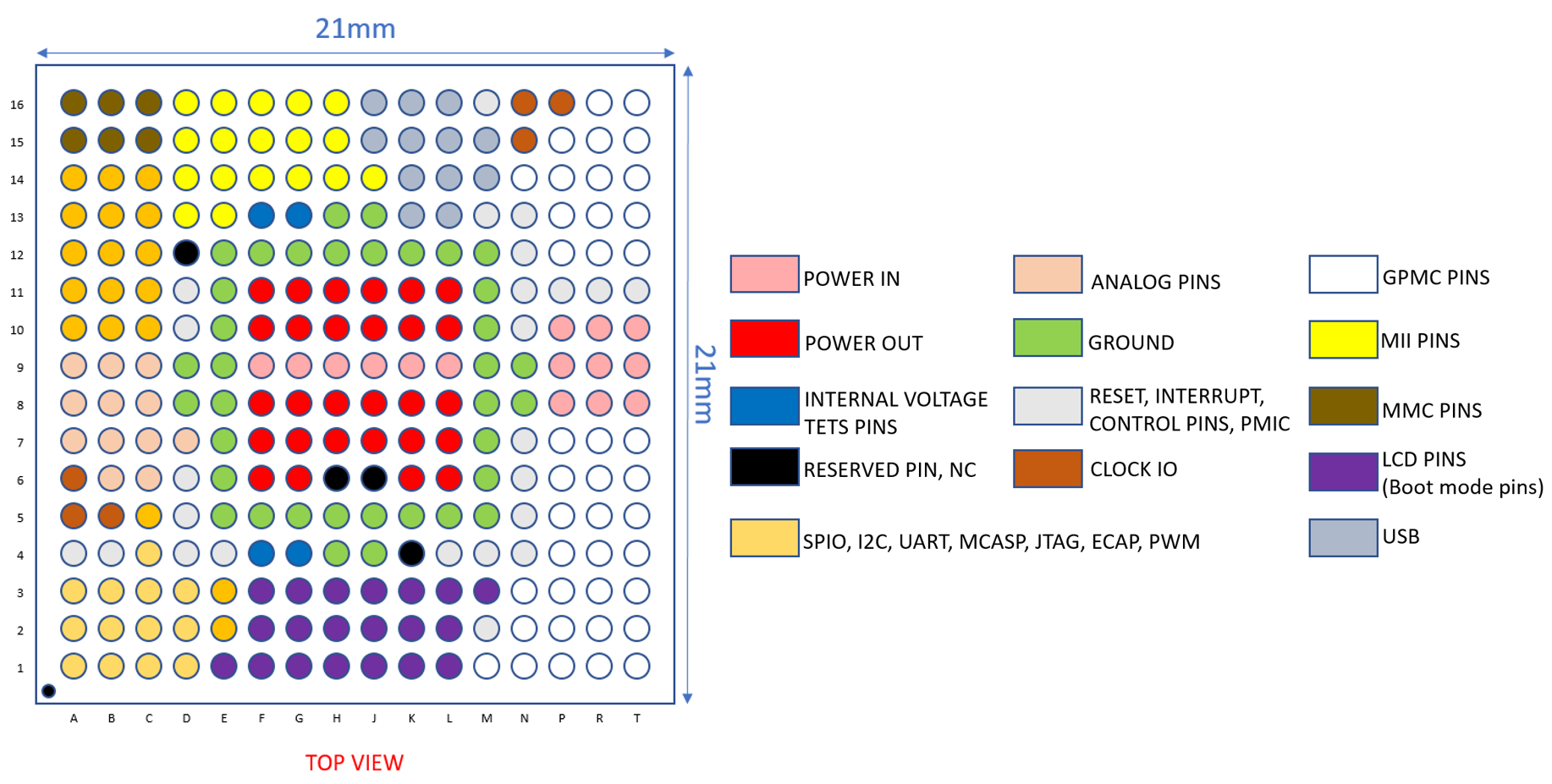
1.2 Ball function map
The Ball function map shown in Figure 1 provides a visual representation of the arrangement of the pins of the OSD335x-SM. This can help with the placement and orientation of the OSD335x-SM in a design.
1.3 Footprint Configuration
The OSD335x-SM footprint parameters are shown in Figure 2 and listed in Table 1.
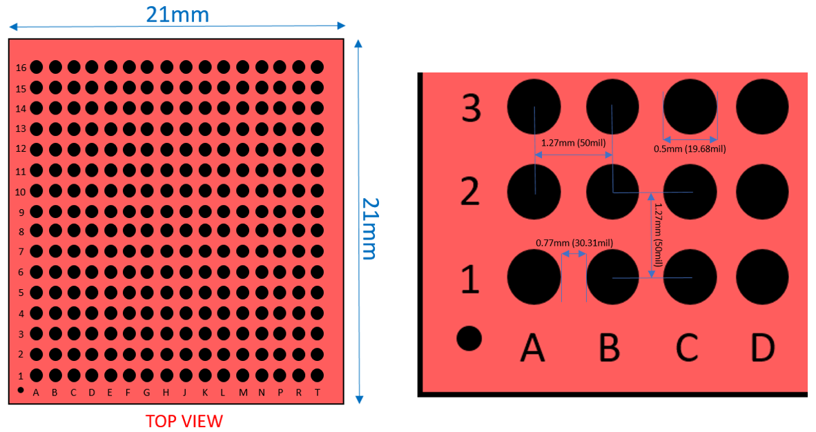
| Parameter | Value |
| Package Dimension | 21mm x 21mm x 2mm |
| Number of Balls | 256 |
| Ball Grid | 16 rows x 16 columns |
| Ball Pitch | 1.27mm (50mils) |
| Landing Pad Size | 0.5mm (19.685mils) |
The landing pad size was determined from the IPC-7351A specification. To find more information about IPC-7351A specifications, refer BGA Ball Pad Size section of BGA PCB Design document from Texas Instruments (TI).
For more information on the footprint configuration, please see the Mechanical Dimensions section of the OSD335x-SM datasheet.
2. Routing and Vias
When pricing a PCB, the size of the traces and vias directly affect the cost to manufacture the board. However, larger traces and vias, while cheaper, can make layout more difficult. Therefore, it is necessary to understand the optimum size of traces and vias for a given design. This section will provide background information on trace and via sizes and discuss layout tradeoffs when designing with the OSD335x-SM BGA.
2.1 Trace size background information
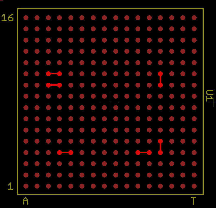
The number of traces that can pass between any two pads of a BGA footprint depends on the trace width and trace spacing. Trace width is the actual width of the trace. Trace spacing is the distance between the edges of any two adjacent traces or a trace and a pad. Trace width and trace spacing are shown pictorially in Figure 3.
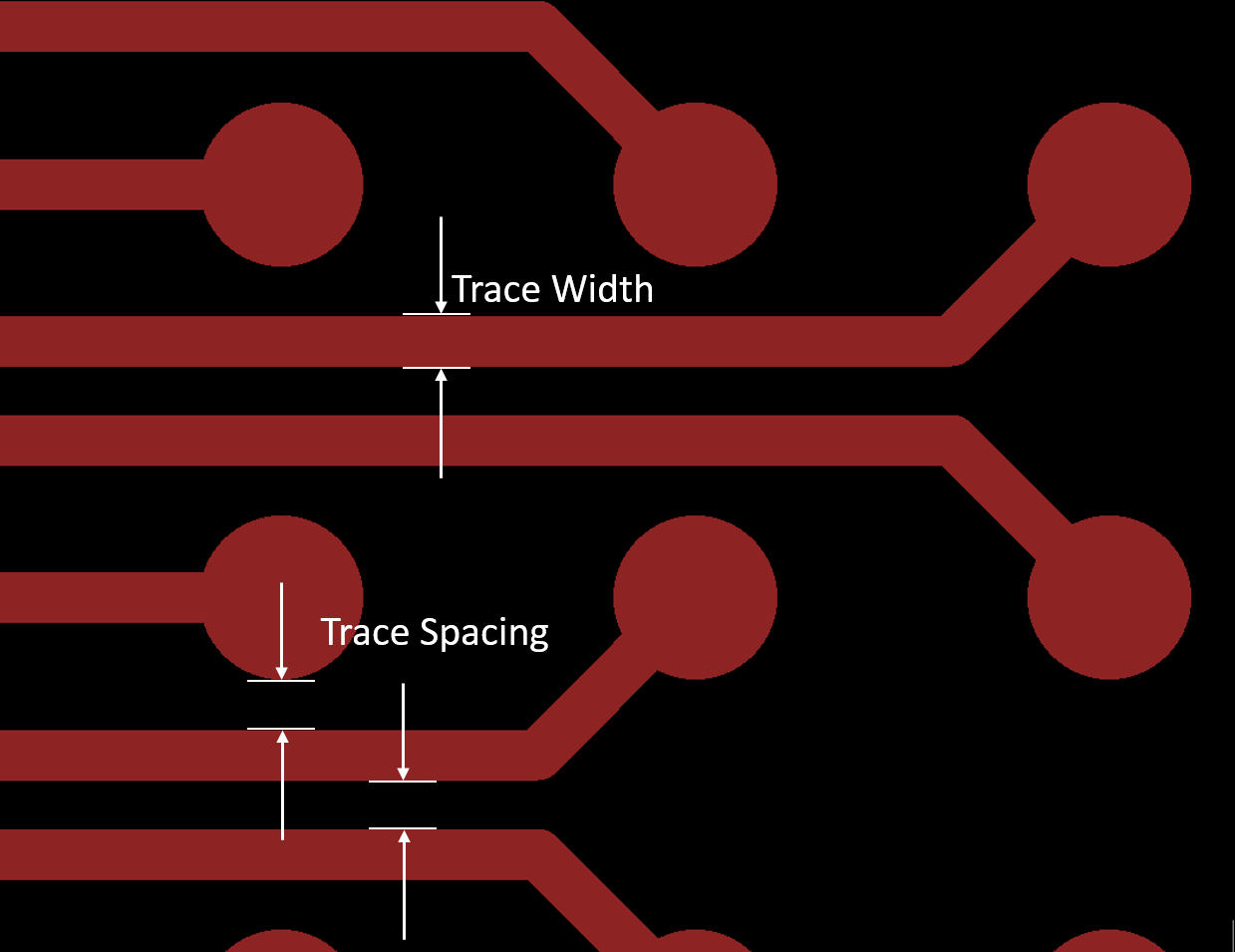
In this document, a “x/y trace” indicates a PCB that uses design rules with trace width of x mils and trace spacing of y mils. For example, a 5/6 trace indicates a PCB with trace width of 5mils and trace spacing of 6mils.
The number of traces that can be routed between any two adjacent pads of the BGA can be calculated using the formula (formula assumes all the traces are equal width):
tn tw + (tn + 1) ts <= BP – BD
where,
tn = number of traces
tw = trace width
ts = trace spacing
BP = BGA pitch
BD = BGA ball diameter
For example, to calculate the number of 6/6 traces that can be routed between adjacent pads of the OSD335x-SM BGA: tw = 6mils, ts = 6mils, BP = 50mil (1.27mm) and BD = 19.68mil (0.5mm)
Using all this in the above equation:
6tn + 6(tn + 1) <= 30.32
12tn <= 24.32
tn <= 2.026 traces.
This result indicates that two (2) full 6/6 traces can be routed between adjacent balls of the OSD335x-SM BGA. Similarly, the number of traces can be calculated for other routing rules, see Table 2. In the OSD335x-SM BGA, almost all signal pins are in the first three rows / columns of the BGA. This means to fully escape the BGA, only 2 traces are needed to be routed between each pair of pads. See Section 4.2 for more details on OSD335x-SM fanout.
| Trace width(mils) / Trace spacing(mils) | Number of traces between two adjacent BGA pads |
| Larger than 6/6 | 1 |
| 6/6 or 5/5 | 2 |
| 4/4 or smaller | 3 or more |
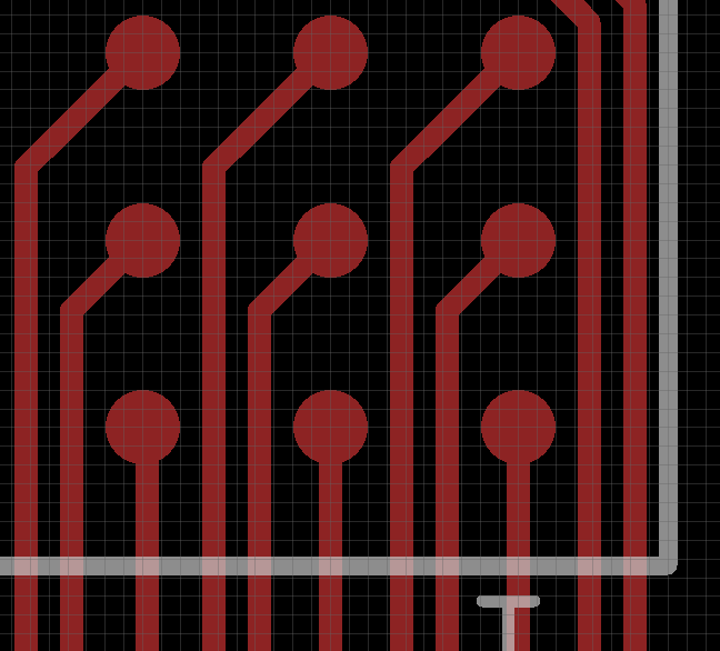
2.1.1 Example: 6/6 traces routed between pads of the OSD335x-SM
On all sides, the first three rows of OSD335x-SM can be easily accessed using 6/6 traces as shown in Figure 4.
2.2 Via size background information
There are two important parameters for vias: drill diameter and annular ring thickness. Drill diameter is the diameter of the actual drilled hole in the PCB. The annular ring thickness is the thickness of the pad that surrounds the drilled hole. These dimensions are shown pictorially in Figure 5.
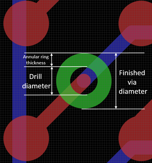
To determine the diameter of the finished via, use the following formula:
Finished via diameter = Drill diameter + 2 x (Annular ring thickness)
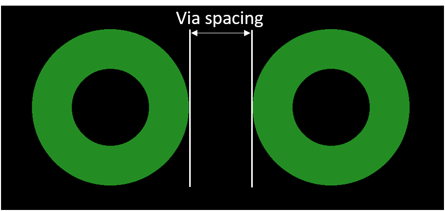
Via spacing is the distance between the edges of any two adjacent vias as shown in Figure 6. When placing vias, make sure the spacing between the vias match the trace spacing design rules that were chosen.
In this document, a “x/y via” indicates a via with drill diameter of x mils and finished via diameter of y mils. For example, a 12/24 via indicates a via with drill diameter of 12mils and finished via diameter of 24mils.
2.2.1 Example: A 12/24 via between 4 pads of the OSD335x-SM
One 12/24 via can be easily placed between four adjacent balls of the BGA as shown in Figure 7.

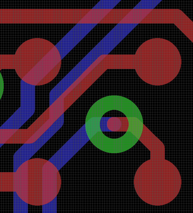
2.2.2 Example: A 12/24 via and 6/6 trace between 4 pads of the OSD335x-SM
Figure 8 shows one 12/24 via and one 6/6 trace between four adjacent pads of OSD335x-SM.
2.2.3 Example: Two 10/18 vias between four pads of the OSD335x-SM
In case of a tighter design, two 10/18 vias can be placed between four adjacent balls of the BGA as shown in Figure 9.

3. OSD335x-SM Layout Examples
Once the design rules for traces and vias have been chosen for the PCB, the BGA can now be routed. The following sections provide examples of how to lay out the OSD335x-SM.
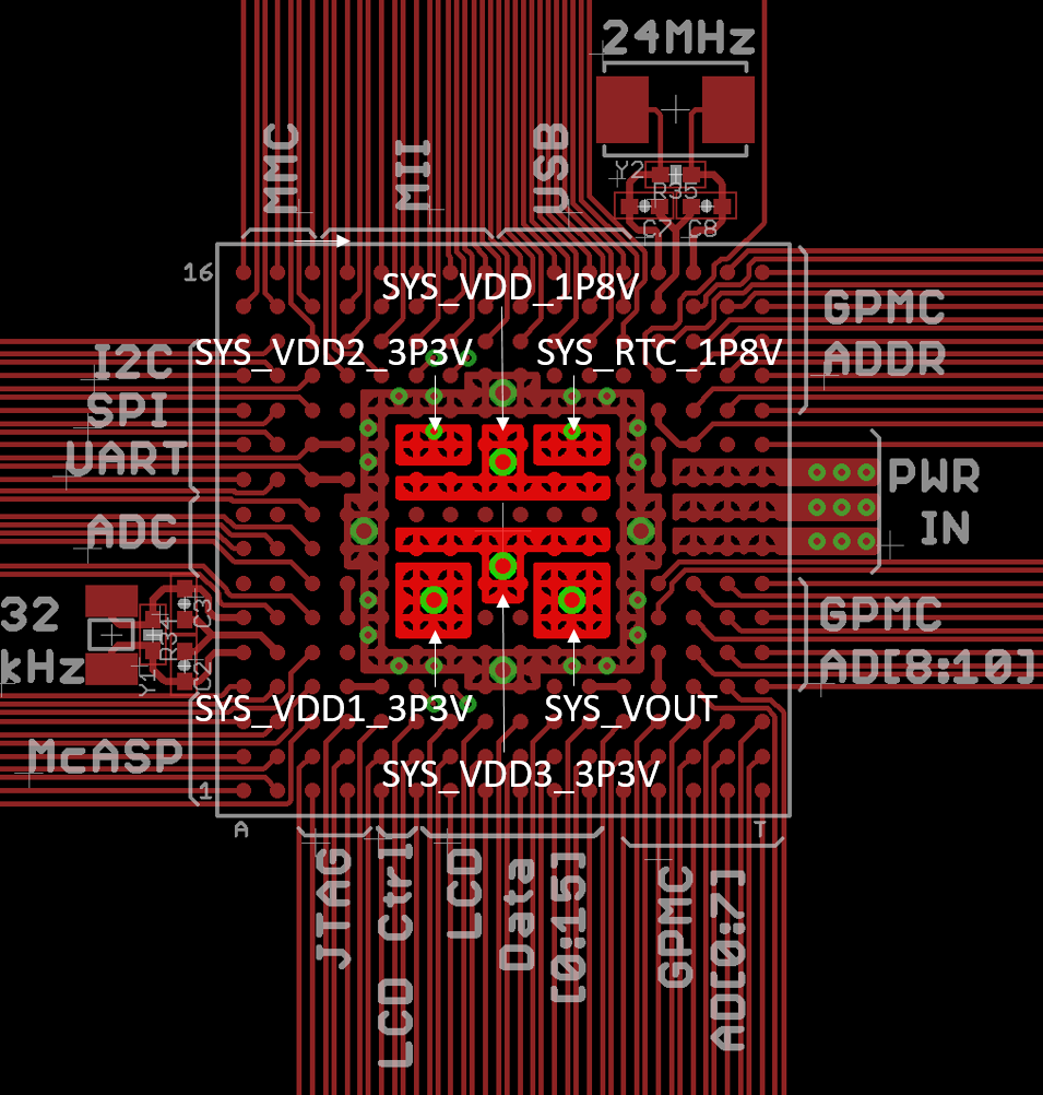
3.1 Mandatory external connections
Figure 10 shows the six external connections (defined in the Minimum connections section of the OSD335x-SM datasheet) that are mandatory for the normal operation of the OSD335x–SM. The I2C interface and PMIC control and status sections of the OSD335x Power Management article has more information about these connections.
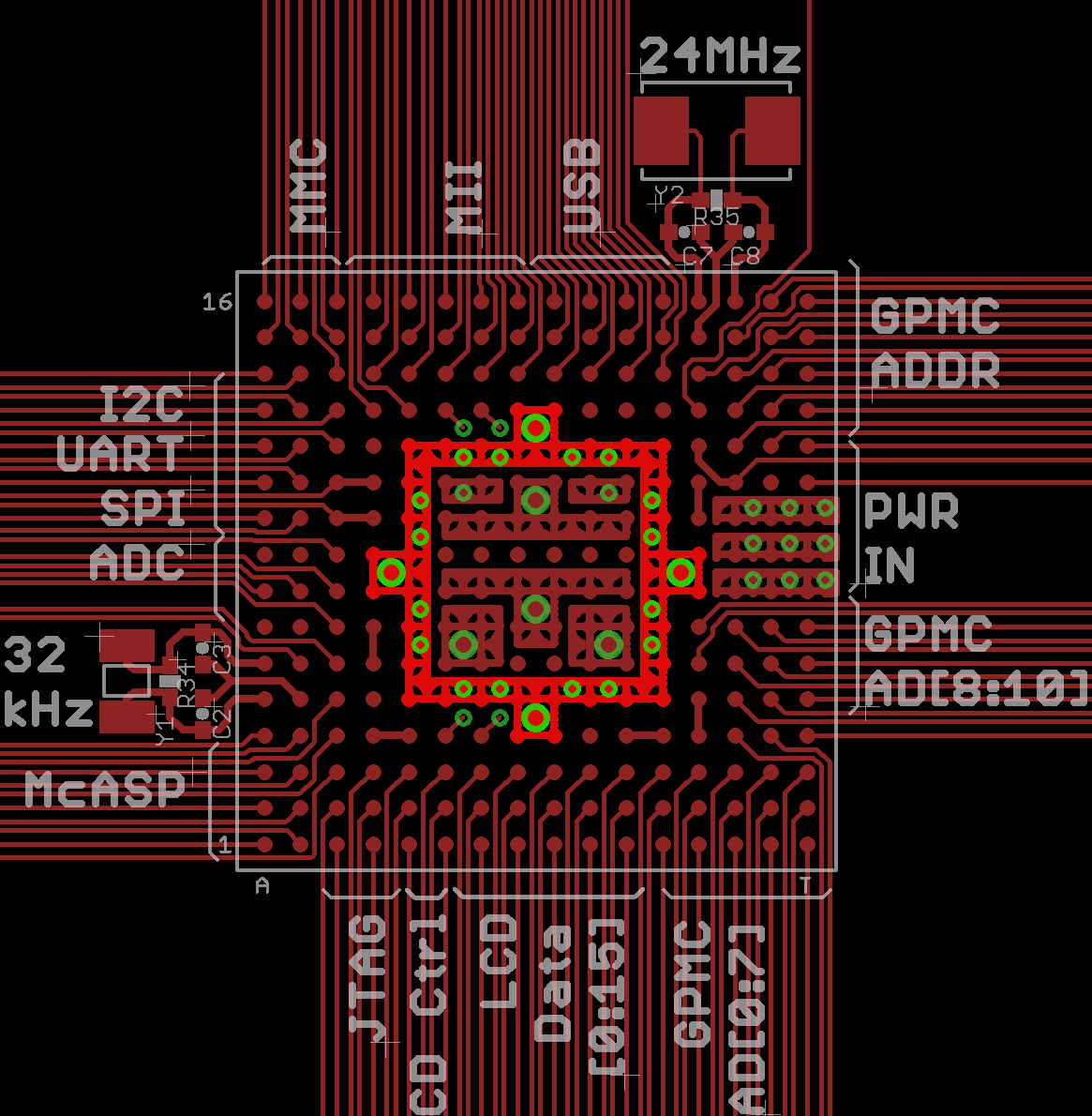
3.2 Signal Pin Fanout
Figure 11 shows the fanout of all pads of the OSD335x-SM using 6/6 traces.
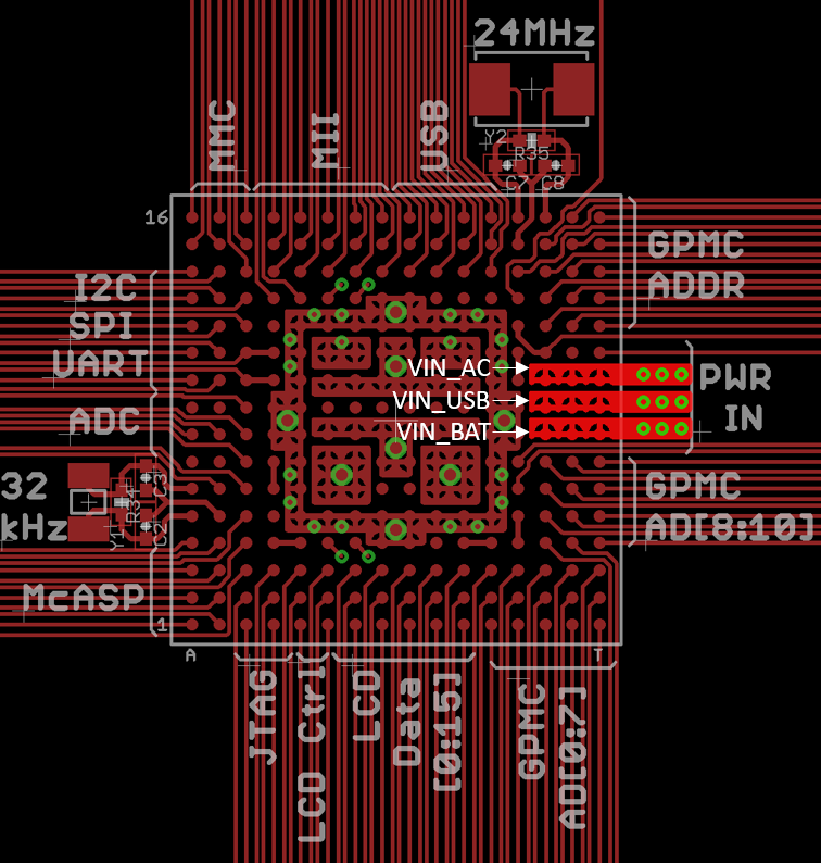
3.3 Power Inputs
Power to the three input power rails (VIN_AC, VIN_USB and VIN_BAT) can be connected to the OSD335x-SM through copper pours as shown in Figure 12.
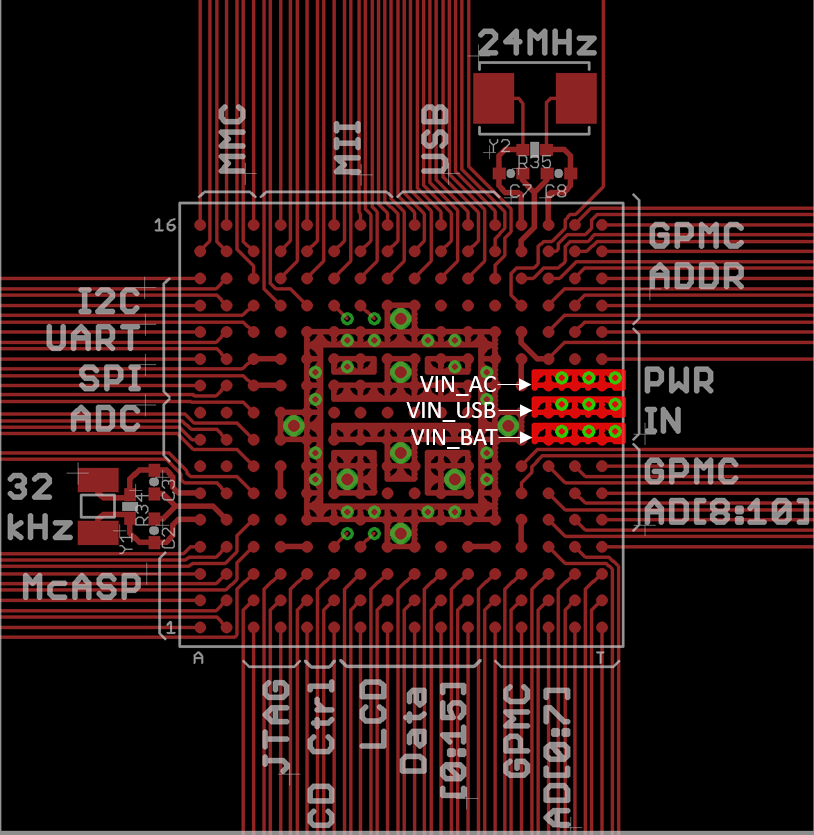
In space constrained designs, smaller input power pours can be used as shown in Figure 13.
3.4 Power Outputs
Power from the output power rails of the OSD335x-SM can be connected to the rest of the PCB using copper pours as shown in Figure 14.
In space constrained designs, the output power copper pours can also be configured as shown in Figure 15.

3.5 Ground connections
The ground pins of the OSD335x-SM can be connected to ground plane using copper pours as shown in Figure 16.

For space constrained design, the ground copper pours can also be configured as shown in Figure 17.
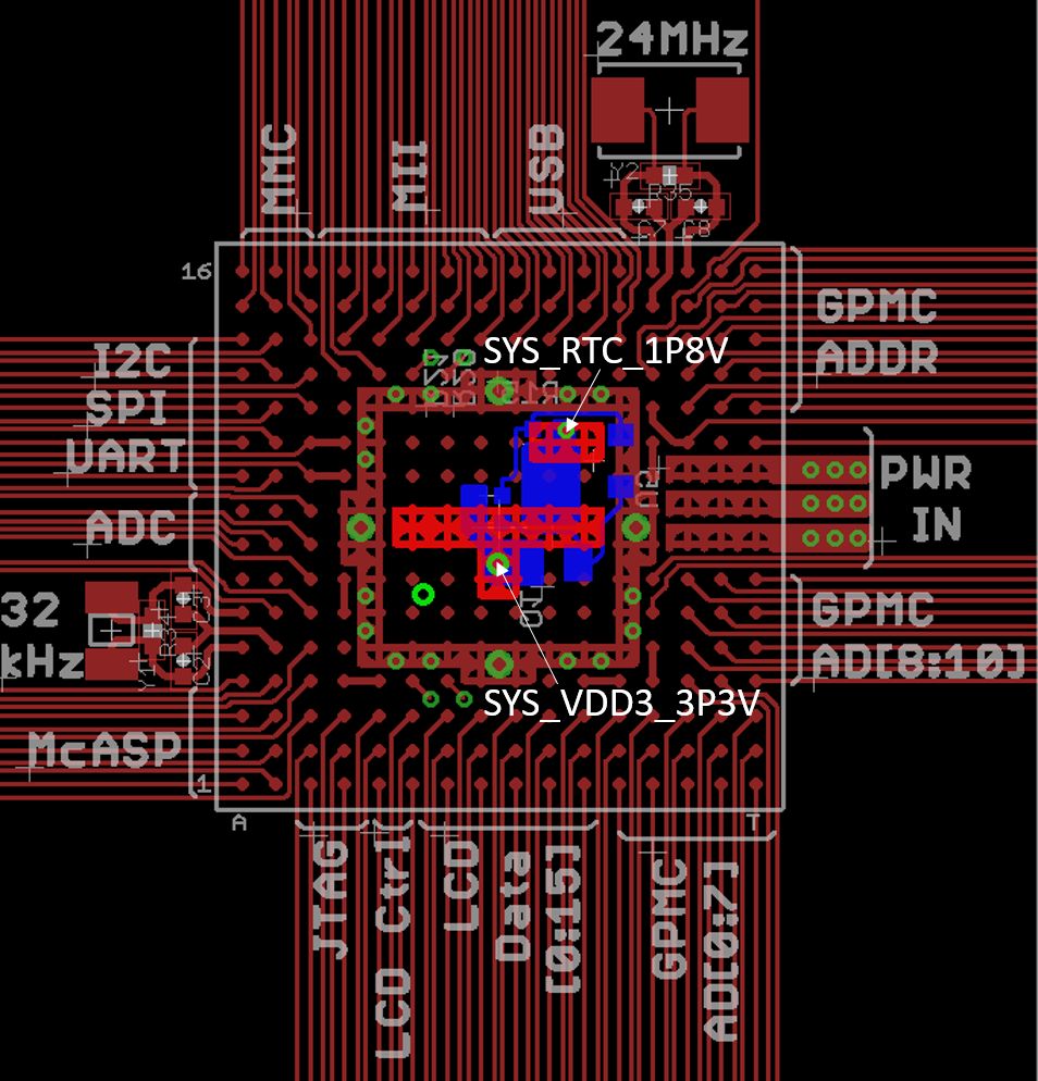
3.6 Clamping circuit
A clamping circuit may need to be connected between the SYS_RTC_1P8V and SYS_VDD3_3P3V rails in the design. More information about the necessity of using the clamping circuit can be found in the OSD335x Clamping Circuit article.
If used, the clamping circuit can be placed directly below the OSD335x-SM on the bottom layer of the PCB. It can be connected to SYS_RTC_1P8V and SYS_VDD3_3P3V through vias as shown in Figure 18.
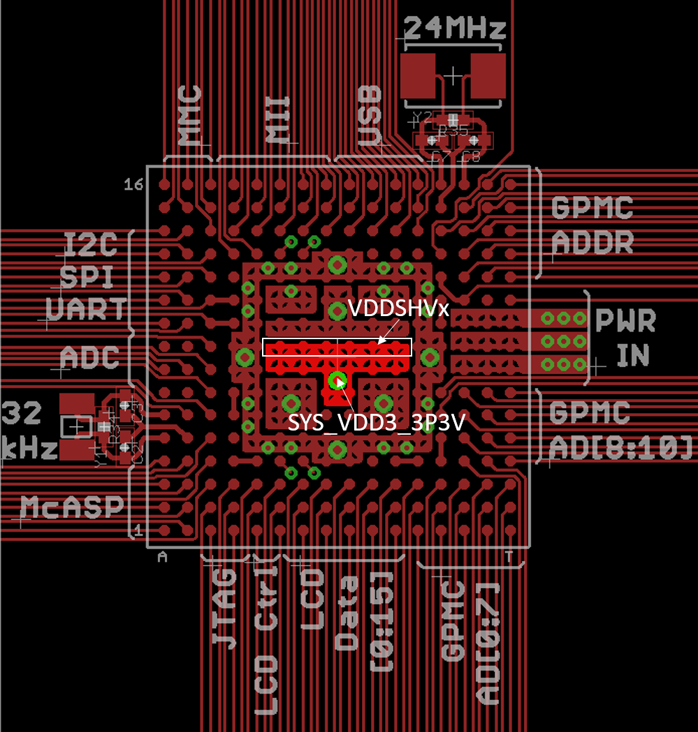
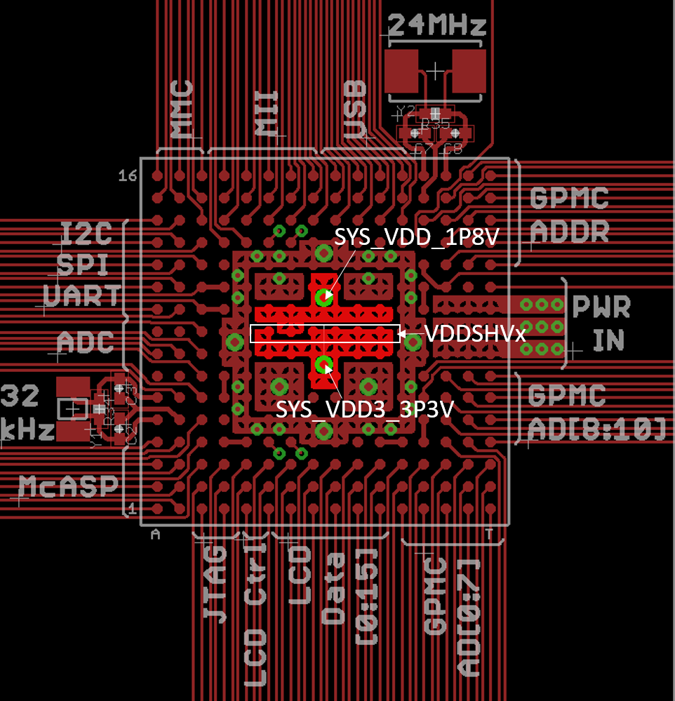
3.7 IO Voltage Connections
The OSD335x-SM I/O domains can operate at either 1.8VDC or 3.3VDC.
The VDDSHVx signals should be connected to the SYS_VDD3_3P3V output voltage rail to set the I/O domains to operate at 3.3V. This can be done using copper pours as shown in Figure 19.
The VDDSHVx pins can alternately be connected to SYS_VDD_1P8V for 1.8V I/O operation using copper pours as shown in Figure 20.

The VDDSHVx pins can also be connected individually to either SYS_VDD3_3P3V or SYS_VDD_1P8V using copper pours. Figure 21 shows an example where VDDSHV5 is connected to SYS_VDD_1P8V for 1.8V operation while the other VDDSHV pins are connected to SYS_VDD3_3P3V for 3.3V operation.
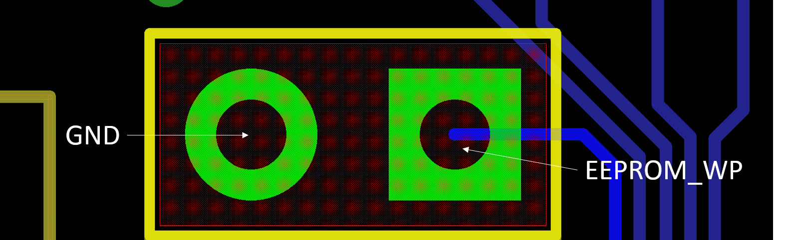
3.8 EEPROM
The write protect pin of the EEPROM (EEPROM_WP) of the OSD335x-SM needs to be driven low before information can be written into it. This can be done in a many ways: The EEPROM_WP pin can be driven by another device on the PCB; It can be driven by one of the OSD335x-SM pins; It can be routed to a pad to be driven by an external device; It can be routed to a jumper; etc.
Figure 22 shows an example of the EEPROM_WP pin routed to a jumper using 100mil header. The other side of the jumper is connected to GND which allows the EEPROM_WP signal to be easily driven low. This can be a useful layout in prototype designs that are not space constrained.