OSD335x Power Management
Published On: August, 1, 2017 By: Eshtaartha Basu | Updated: July 18, 2018 by Cathleen Wicks
Introduction
This article is the third part of the OSD335x Reference Design Lesson 1 Power circuitry articles. It will mainly focus on topics related to control and management of power for the OSD335x. As we discuss the power circuitry, we will build the schematics and layout the corresponding traces.
Prerequisite
This article is a part of the broader OSD335x Reference Design Lesson 1 series which consists of a sequence of articles designed to help you build the bare minimum circuitry required to boot the OSD335x.
We recommend reading the second part of power circuitry article OSD335x Ground Connections before this one. This article builds upon the foundation outlined in it.
All design files for this lesson can be downloaded here.
This articles as well as the entire OSD335x Design Tutorial can be downloaded here.
I2C interface
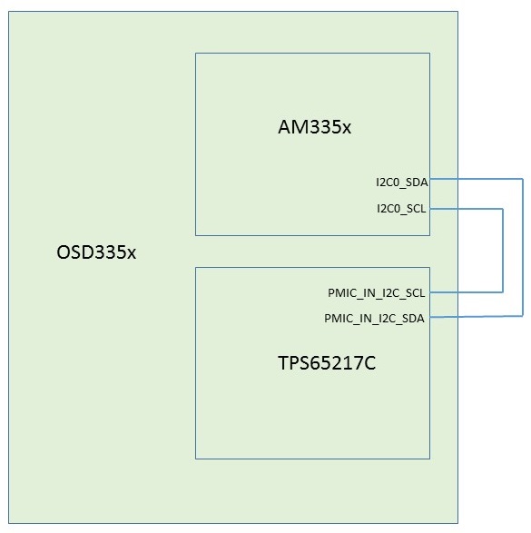
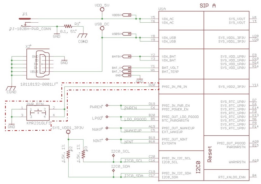
For most designs, the AM335x processor communicates with the TPS65217C PMIC through the I2C0 interface. Therefore, the I2C lines for both the processor and the PMIC are brought out to the BGA balls of the OSD335x to give flexibility in how things are connected. Almost always, the I2C0 pins of the AM335x and the I2C pins of the TPS65217C PMIC are connected externally to enable I2C communication between the processor and PMIC. The I2C pins that need to be connected are placed close to each other on the OSD335x schematic symbol to facilitate easy connection. The necessary connections are shown in Figure 1 block diagram.
The I2C0 pins of the AM335x processor have internal 4.7K ohm pullup resistors. This is sufficient if nothing else is connected to the I2C0 bus. In the case that other components are connected to the I2C0 bus, it is good practice to put additional external pull-up resistors. This allows the strength of the pull-ups on the I2C0 bus to be set based on the other bus components. For this design, given we are connecting to some unknown components, we are going to use 1.5k ohm external pull-ups whose value can be adjusted later if necessary.
Most of the functionality of the TPS65217C PMIC can be controlled and various parameters can be set using the I2C interface. Some of the features that can be controlled are:
- Battery charger voltage.
- Charge safety timer control.
- Buck and Boost converter output voltage.
- LDO output voltage.
- Power up and power down sequences.
- Over current and over temperature thresholds.
Details about the I2C interface and its usage can be found in the TPS65217C datasheet.

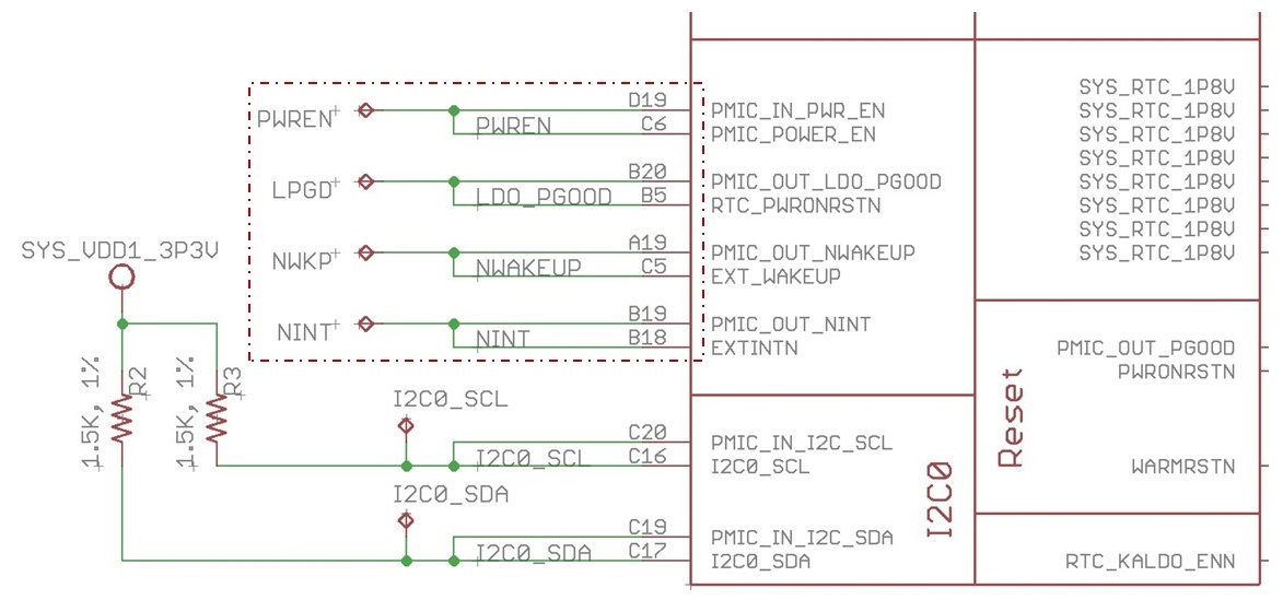
Let’s make I2C connections on the schematic as shown in Figure 2 (Updates made to the schematics are shown using dotted lines).
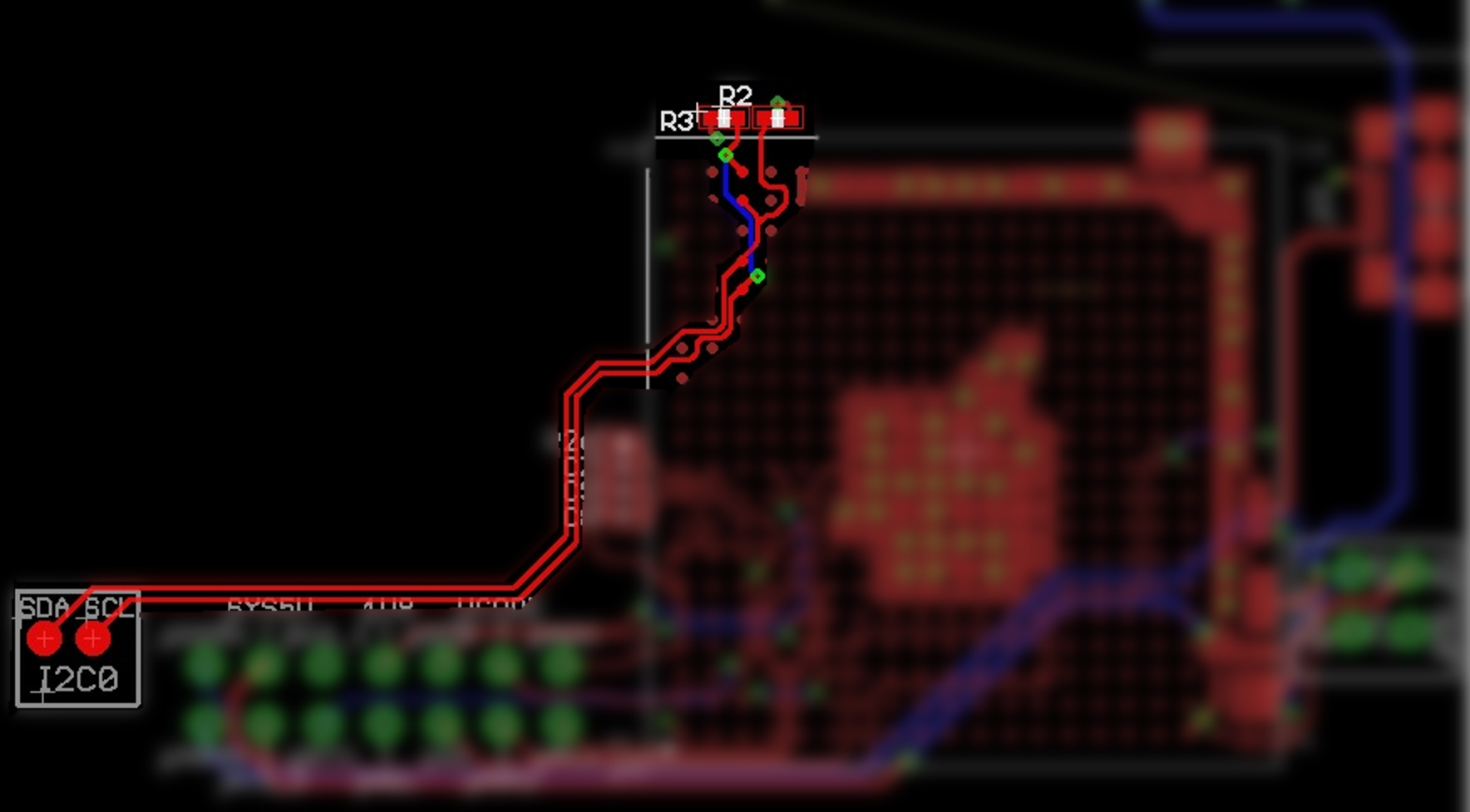
The highlighted routes in Figure 3 represent the I2C connections in the layout.
PMIC control and status
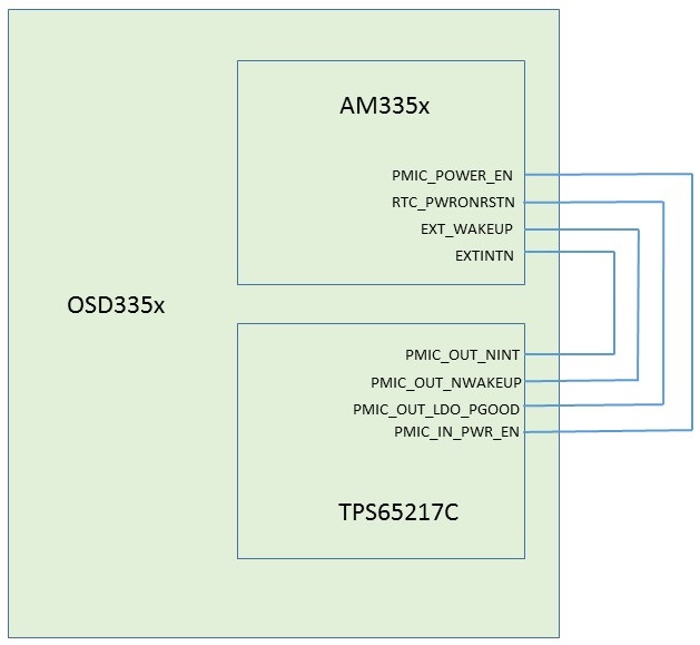
Besides the I2C connections, there are a few more signals that must be connected between the processor and PMIC for the OSD335x to function correctly. Figure 4 shows the external signal connections that we must make to allow the AM335x and the TPS65217C PMIC to coordinate their operations. These signals were brought out of the OSD335x so that the user can have more control over power sequencing if necessary. The description of these signals are:
- PMIC_POWER_EN: This pin is used by the AM335x to control the power up sequence of the PMIC.
- PMIC_IN_PWR_EN: Enable input for buck converters and LDOs on the PMIC. Pulling this pin high will start the power up sequence.
- RTC_PWRONRSTN: Independent Power On Reset Pin of the AM335x RTC.
- PMIC_OUT_LDO_PGOOD: LDO power good output. This pin goes high when both LDO1 and LDO2 output voltages are within regulation and goes low when either one of them are out of regulation.
- EXT_WAKEUP: Dedicated input pin of the AM335x for external wake up events.
- PMIC_OUT_NWAKEUP: Signal to host to indicate a power on event (active low)
- EXTINTN: External interrupt input of the AM335x.
- PMIC_OUT_NINT: Interrupt output (active low) of the PMIC.
For this design, we do not need any additional control of the power sequencing, so we can directly connect the pins. However, let’s add test points so that we can probe these signals during bring-up. Let’s make the necessary connections on the schematic as shown in Figure 5 (Updates made to the schematics are shown using dotted lines).
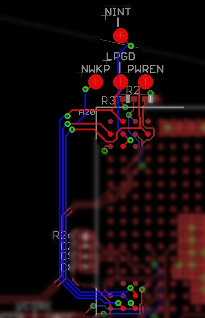
The highlighted routes in Figure 6 represent the PMIC control and status connections in the layout.
Power button
The TPS65217C PMIC inside the OSD335x has an active low reset input which is brought out through the PMIC_IN_PB_IN pin of the OSD335x and can be connected to a push button. This input has a 50ms deglitch time and an internal pull-up resistor to an always-on supply. Furthermore, the power button has the following functions:
- The PMIC will be powered up from OFF or SLEEP mode upon detecting a falling edge on PMIC_IN_PB_IN.
- PMIC is power cycled/reset when PMIC_IN_PB_IN is held low for more than 8 s. All rails will be shut down by the sequencer and all register values are reset to their default values. Rails not controlled by the sequencer are shut down immediately. The device remains in this state for as long as this pin is held low. However, the device will remain in RESET state for a minimum of 1 second before it returns to ACTIVE state.
- If the PMIC_IN_PB_IN pin is kept low for an extended amount of time, the device will continue to cycle between ACTIVE and RESET state, entering RESET every 8 seconds.

You can find more information about power button and PMIC modes at:
http://www.ti.com/product/TPS65217/datasheet/detailed-description#SLVSB641234
http://www.ti.com/product/TPS65217/datasheet/detailed-description#SLVSB643180
The schematic is developed as shown in Figure 7 (Updates made to the schematics are shown using dotted lines). The power button we’re using can be found under the device name KMR231GLFS in the given library.

Long-pressing the power button on some boards will power off the system instead of power cycling it. This state occurs when the TPS65217C PMIC shuts off SYS_5V at the start of the power down sequence. If the SYS_5V rail powers down before the regulated supplies, which it powers, it can result in a PMIC fault. This causes the system to go to the OFF-state instead of going through the normal power-cycle sequence.
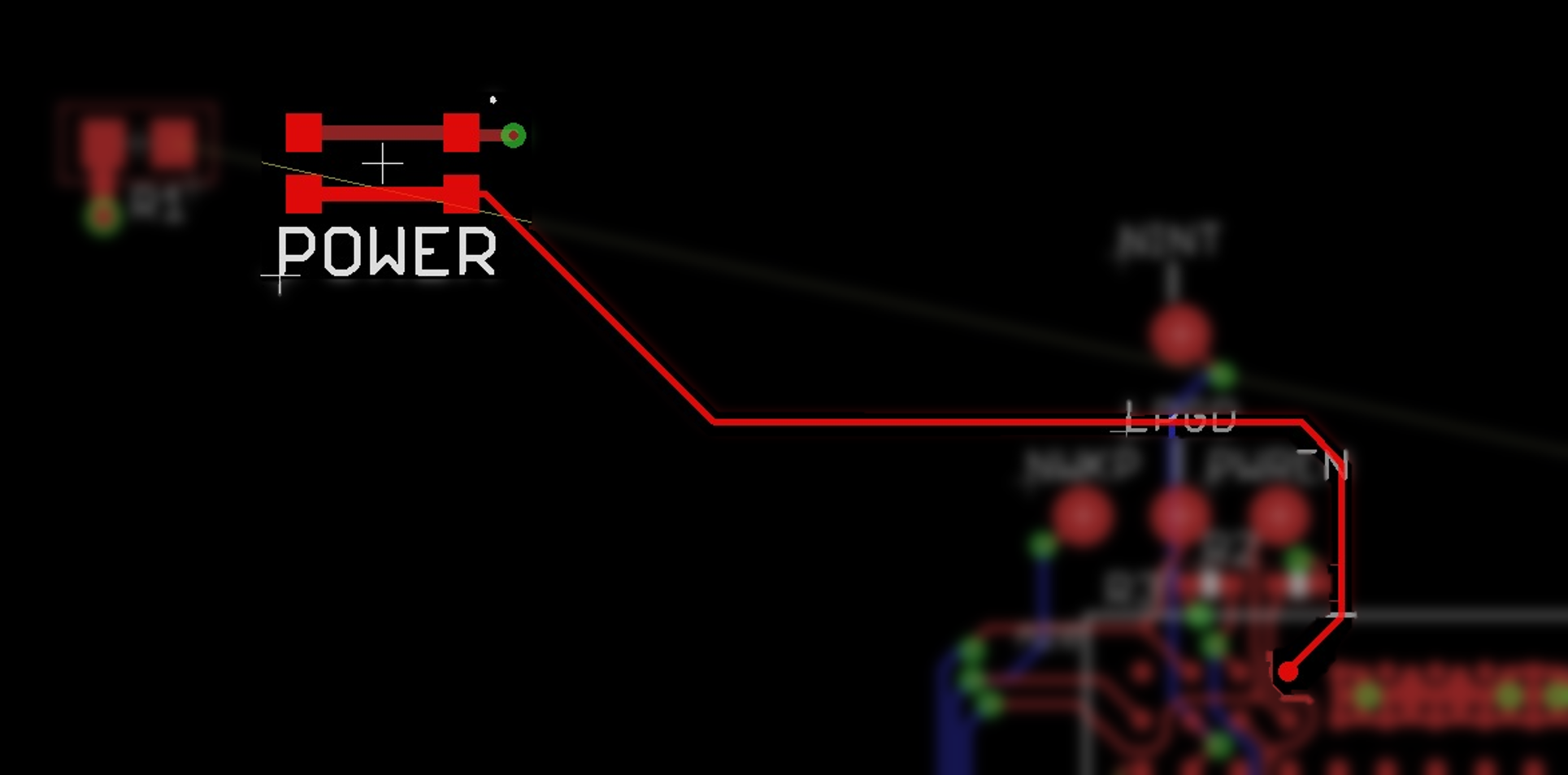
The highlighted routes in Figure 8 represent the power button connections in the layout.
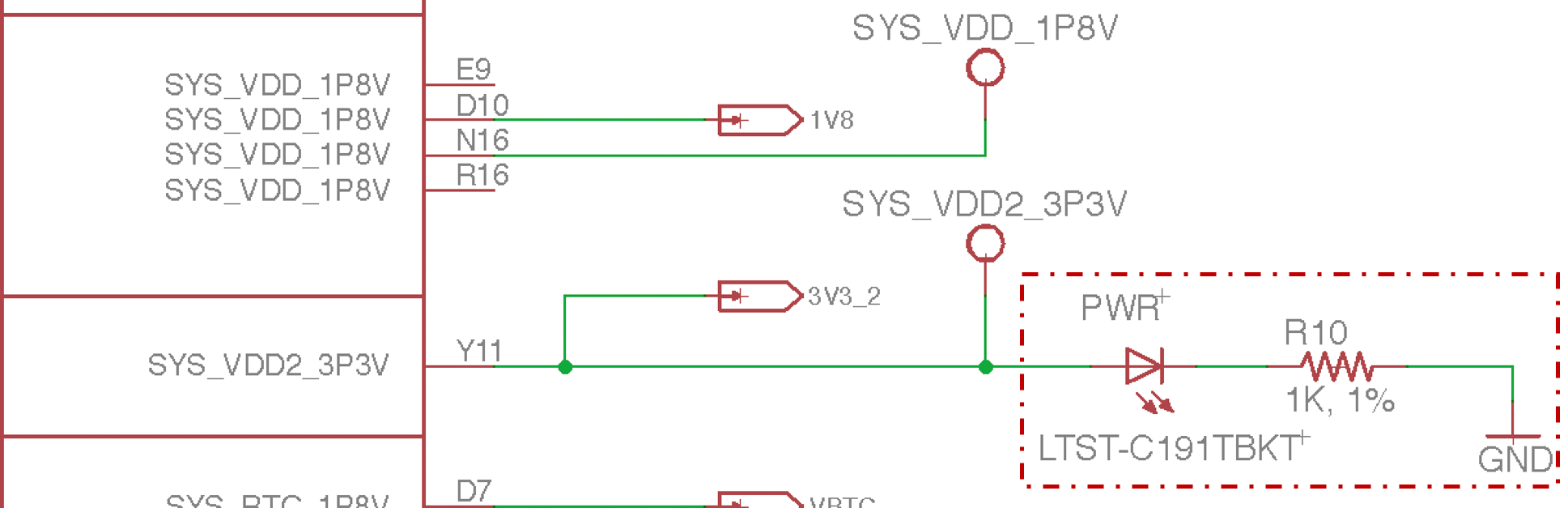
Power indicator LED
For this design, we want to have an LED to indicate that power is on. Since SYS_VDD2_3P3V can only supply 150mA externally, we used this power output to indicate power is on as shown in Figure 9 (Updates made to the schematics are shown using dotted lines).
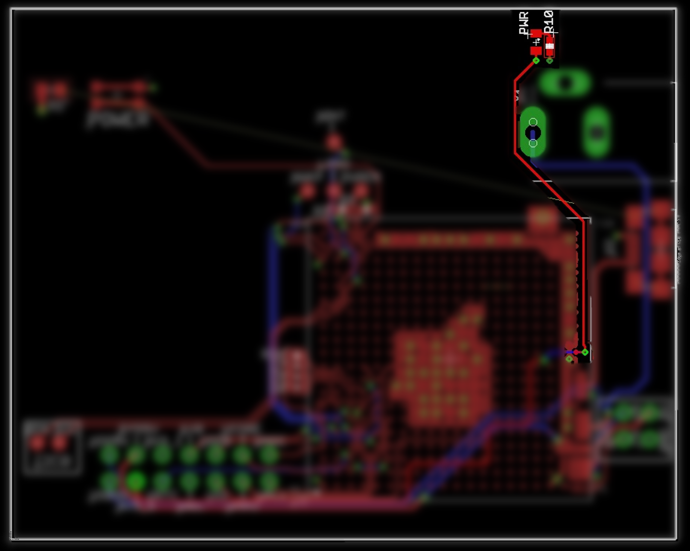
The highlighted routes in Figure 10 represent the power LED connections in the layout.
| << Return to “OSD335x Ground Connections” | Continue to “OSD335x Clamping Circuit” >> |
