OSD335x Reset Circuitry
Published On: August, 2, 2017 By: Eshtaartha Basu | Updated: September 30, 2020 by Greg Sheridan
Introduction
This article will help you understand the OSD335x Reset Circuitry design methodology.
A Reset circuit/pin is typically used to help a microprocessor reinitialize itself and resume its normal operation whenever it runs into an error condition which is undesirable for the current activity and when all other recovery mechanisms fail. It is also used during power-up to make sure the microprocessor and all its modules start their operation from a known state.
Prerequisite
This article is a part of the broader OSD335x Reference Design Lesson 1 series which consists of a sequence of articles designed to help you build the bare minimum circuitry required to boot the OSD335x.
We recommend reading the article OSD335x ESD Protection before this one. This article builds upon the foundation outlined in it.
All design files for this lesson can be downloaded here.
This articles as well as the entire OSD335x Design Tutorial can be downloaded here.
Reset Types
Before we jump into the OSD335x specifics, let’s look at the type of reset inputs typically provided by Texas Instruments (TI). TI generally provides two types of resets: Cold Reset and Warm Reset. Let’s look at the properties of both these reset types:
Cold reset
- It affects all the logic within the given entity (sub-system, module or macro-cell).
- It is non blockable (This signal cannot be interrupted or blocked using software or any other internal module. Once this signal is triggered, the device immediately performs all the necessary operations irrespective of its state).
- A cold reset takes place during device power-up and power domain power-up.
- Cold reset is synonymous with Power-On-Reset.
Warm reset
- It is a partial reset which doesn’t affect all the logic within the given entity.
- It is used to reduce Reset recovery time (Time required to resume normal operation after application of reset signal).
In general, a reset signal is asserted during device startup to make sure the device begins operation from a known initial state each time it is powered up. This signal is applied until the power supplies are stable and the device can begin normal operation. A reset signal is also applied during device operation when the microprocessor runs into an error condition which is undesirable for the current activity and all other error recovery mechanisms fail.
The OSD335x provides three reset inputs PWRONRSTN, WARMRSTN and RTC_PWRONRSTN which are directly connected to the AM335x processor reset inputs of the same name. Let’s look at each of them in more detail:
PWRONRSTN
- It is a cold reset.
- It needs to be driven low during device power-up until all the input power lines have ramped up and are stable.
- It is non blockable (PWRONRSTN signal cannot be interrupted or blocked using software or any other internal module. Once this signal is triggered, the device immediately performs all the necessary operations irrespective of its state).
- Entire system is affected except RTC (Real Time Clock) module.
- SYSBOOT (boot configuration) pins are latched when reset is de-asserted.
WARMRSTN
- It is a warm reset.
- It can be blocked by EMAC (Ethernet Media Access Controller) switch.
- PLLs are not affected.
- Most debug logic subsystems are not affected. This allows us to maintain debug session even after warm reset event.
- SYSBOOT pins are not latched with warm reset.
- Some PRCM (Power, Reset and Clock Management) and control module registers are warm reset insensitive.
- Warm reset assumes power supply and clock is stable from assertion through de-assertion.
RTC_PWRONRSTN
- Dedicated Power-On-Reset input for the RTC module.
- RTC module is not affected by device Power-On-Reset (PWRONRSTN). Similarly, RTC_PWRONRSTN will not have any effect on the rest of the device.
Reset external connections
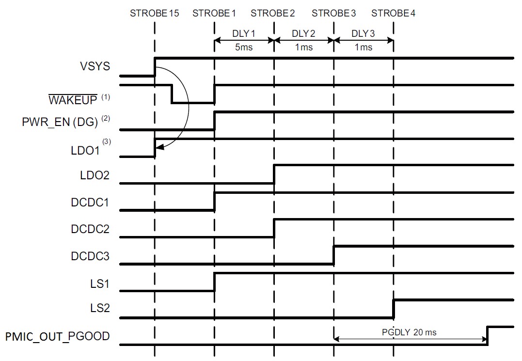
During power-up, voltages on the input power rails of the AM335x processor will be ramping up as shown in Figure 1 (More information about Power-Up sequence of various power rails can be found in Power-Up Sequencing section of the TPS65217 datasheet). The PWRONRSTN pin should be driven low until all the power rails have ramped up and are stable. The PMIC_OUT_PGOOD pin will be maintained low when power rails are ramping up or when the power on any of the power rails is below the required value. It will go high only when the power on all power rails are stable as shown in Figure 1. Hence, the PWRONRSTN pin needs to be driven by the PMIC_OUT_PGOOD pin. Both the PWRONRSTN and the PMIC_OUT_PGOOD signals are brought out of the OSD335x and they need to be connected externally as shown in Figure 2.
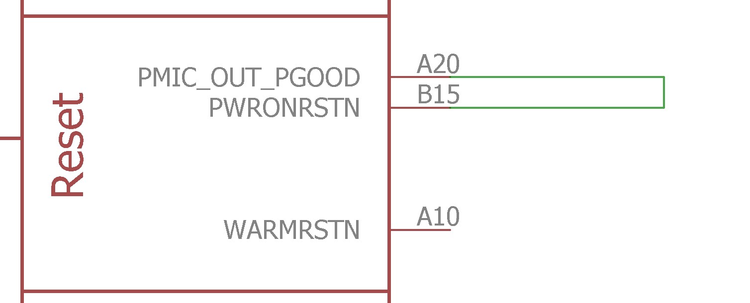
As described in the PORz Sequence section of the AM335x TRM, for the WARMRSTN pin (nRESETIN_OUT) to maintain a valid low state until the supplies are ramped, it should also be driven by PMIC_OUT_PGOOD. However, due to I/O voltage differences (PMIC_OUT_PGOOD and PWRONRSTN pins operate at 1.8V while the WARMRSTN pin operates at 3.3V) and the need for independent reset control, WARMRSTN should be driven by PMIC_OUT_PGOOD thru an open-drain buffer (SN74LVC1G07). For more information on the requirement of open-drain buffer, see section 8.1.7.3.2 PORz Sequence (page 1236) of the AM335x TRM (Rev. P).
To manually reset the OSD335x in the case of a software or hardware error condition, we will also add a push button as a reset source for WARMRSTN. Push buttons are susceptible to ground bounce which may lead to multiple resets or partial resets. To overcome this problem, a reset supervisor circuit can be used. The APX811 is an efficient and cost effective solution which allows us to consolidate the reset sources for WARMRSTN and drive the signal cleanly. The entire reset supervisor circuit can be seen in Figure 3.

- A supervisor circuit (with manual reset input) has two specific functions. It asserts a reset signal for a fixed period of time whenever the:
- supply voltage falls below a preset voltage.
- the manual reset input is asserted. (it may care of input button de-bouncing also)
- You can find more information about APX811’s operation by going through its datasheet here.
If you don’t intend to use a reset supervisor circuit in your design, you can refer to the Reset Circuit section of OSD335x Schematic Checklist to find other ways of building a reset circuit.
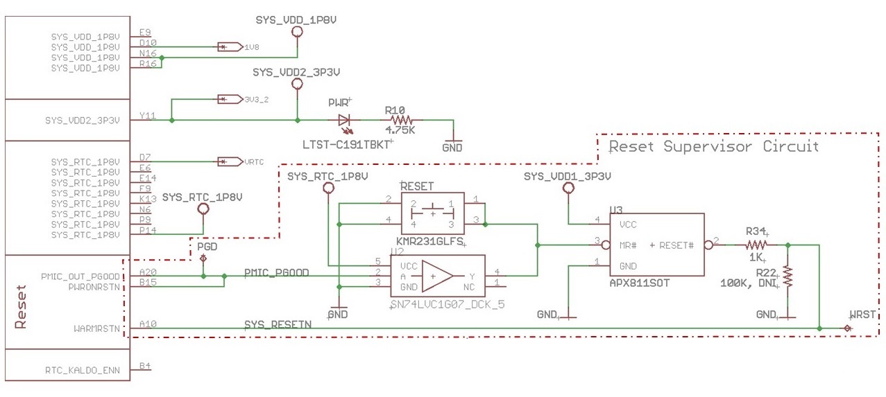
The connections are made as shown in Figure 3 (Schematic updates are shown using dotted lines).
Let’s go layout corresponding traces to complete the reset circuit design process as shown in Figure 4.
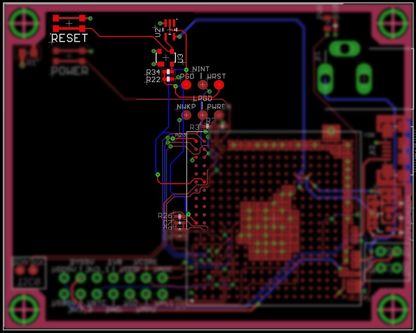
The components are placed in a specific manner to accommodate future components and facilitate easy routing.
| << Return to “OSD335x ESD Protection” | Continue to “OSD335x Clock Circuitry” >> |
