OSD335x Clock Circuitry
Published On: August, 2, 2017 By: Eshtaartha Basu | Updated: October 1, 2020 by Greg Sheridan
Introduction
A clock is essential for the operation of any microprocessor. Therefore, proper design of the clock circuit is pivotal to achieve reliable operation. This article will help you understand the OSD335x Clock Circuitry design methodology.
Prerequisite
This article is a part of the broader OSD335x Reference Design Lesson 1 series which consists of a sequence of articles designed to help you build the bare minimum circuitry required to boot the OSD335x.
We recommend reading the article OSD335x Reset Circuitry before this one. This article builds upon the foundation outlined in it.
All design files for this lesson can be downloaded here.
The OSD335x OSC0 and OSC1
The OSD335x has two clock inputs. They are:
OSC0: This is the High Frequency Oscillator Input. This clock source is also called the Master Oscillator. It operates at either 19.2MHz, 24MHz, 25 MHz or 26MHz. This clock source provides reference for all non-RTC functions. The OSC0_IN, OSC0_OUT and OSC0_GND pins are used for this clock input.
OSC1: This is the Low Frequency Oscillator Input. This clock source provides a reference clock for the Real Time Clock (RTC) and operates at 32.768kHz. The OSC1_IN, OSC1_OUT and OSC1_GND pins are used for this clock input.
OSC1 is disabled by default when power is applied. This clock input is optional and is not required if the RTC (Real Time Clock) module is configured to receive clock from internal 32kHz RC oscillator or if the RTC modules is not needed at all.
For more information on clock sub-systems, you can refer the Clock Management section of the AM335x Technical Reference Manual.
The crystal oscillator circuit for OSC0 is shown in Figure 1.
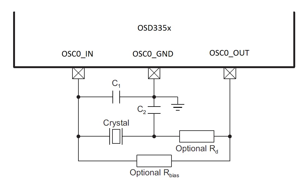
- According to the AM335x datasheet, resistors Rbias and Rd are optional. For the reference design, we added the footprint for Rbias to give us the flexibility to add a resistor to the circuit if the default configuration (i.e. just C1 and C2 are connected) did not provide the desired crystal performance. Additionally, Rbias’s footprint can be left unpopulated if it is not needed since it is in parallel with OSC0_IN and OSC0_OUT pins.
However, Rd is in series with the crystal and the OSC0_OUT pin, so it must always be populated even if it is not needed, which adds cost to the design. We decided not to add the footprint for Rd since we didn’t think we needed it and it makes the layout cleaner.
For the reference design, we were happy with the performance of the crystal when we just used a 1Mohm resistor for Rbias. You will have to decide how to handle Rbias and Rd based on your design and your crystal.
- C1 and C2 represent the total capacitance of the respective PCB trace, load capacitor, and other components (excluding the crystal) connected to each crystal terminal. The value of capacitors C1 and C2 should be selected to provide the total load capacitance, CL, specified by the crystal manufacturer. The total load capacitance is CL = [(C1 × C2) / (C1 + C2)] + Cshunt, where Cshunt is the crystal shunt capacitance (C0) specified by the crystal manufacturer. As long as the layout guidelines are followed, we can assume that the capacitance of the PCB trace and other components is small and can be ignored in the calculation of C1 and C2.
- For recommended crystal circuit component values for OSC0, check OSC0 Crystal Circuit Requirements table in the AM335x datasheet.
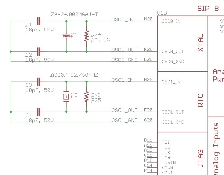
- The AM335x supports either 19.2MHz, 24MHz, 25MHz or 26MHz clock input for OSC0. However, the software we will be using in future lessons assumes a 24MHz input clock. Hence, we will be using 24MHz crystal oscillator 7A-24.000MAAJ-T from TXC for OSC0. Based on the above mentioned guidelines for capacitor selection, we will be using 18pF capacitors for both C1 and C2 for our OSC0 design.

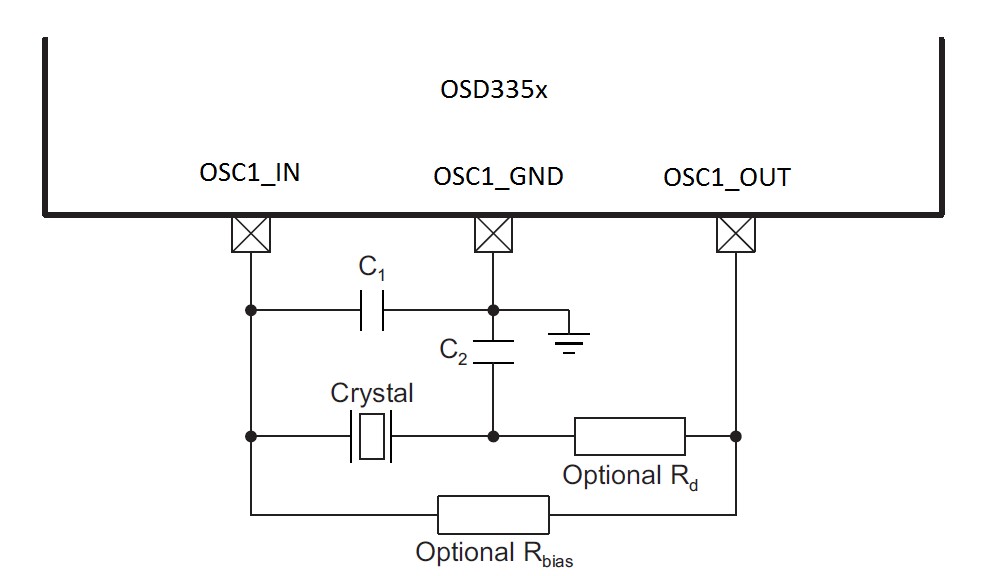
- The crystal oscillator circuit for OSC1 is shown in Figure 2 and is the same as the oscillator circuit for OSC0. For the reference design, we do not need either Rbias or Rd since OSC1 has an internal resistor. However, as discussed above, we have placed a footprint for Rbias but not for Rd to give us the flexibility to adjust the crystal performance without increasing the design cost. For recommended crystal circuit component values for OSC1, check OSC1 Crystal Circuit Requirements table in the AM335x datasheet. OSC1 circuit operates in the same way as OSC0 circuit.
- The AM335x only supports a 32.768kHz clock input for OSC1 input. Therefore, we will be using the 32.768kHz crystal oscillator ABS07-32.768KHZ-T from Abracon LLC for OSC1 design. Based on the guidelines above for capacitor selection, we will be using 18pF capacitors for both C1 and C2 for our OSC1 design.
Now let’s add OSC0 and OSC1 circuits into our schematics as shown in Figure 3.

Layout guidelines
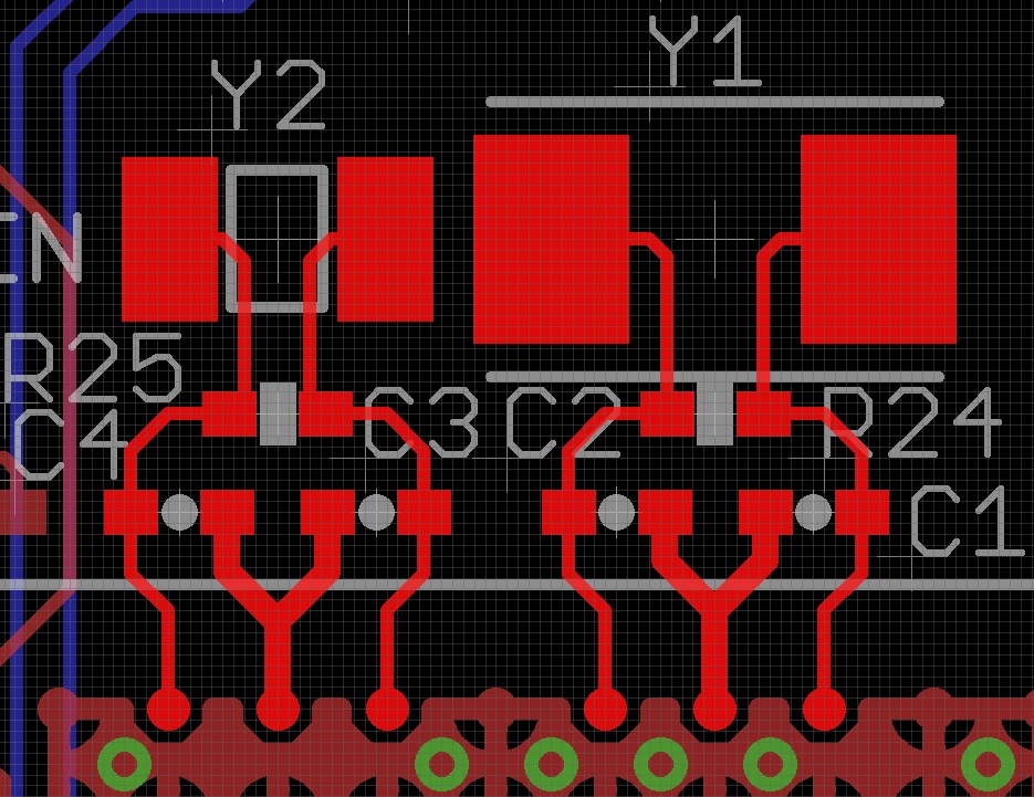
Here are the guidelines we used for crystal oscillator layout in this design:
- The crystal oscillator is sensitive to noise from other signals. Other digital activities on the board may also distort the small amplitude sine wave from the crystal oscillator. Therefore, care should be taken when placing components or routing signals near the oscillator circuit to avoid capacitive coupling.
- The crystal oscillator circuit components should be placed close to the OSD335x.
- For the OSD335x, each oscillator has an oscillator ground. This should be used as the ground reference for the oscillator.
- Try not to route any other signal under the oscillator circuit wherever possible.
- If routing signals under the oscillators, then try to make sure that the signal traces cross at right angles vs running parallel to oscillator traces to minimize coupling.
- Avoid right angle traces.
- Avoid vias for clock signals if possible. If not possible, then make sure that there is enough keep out in the inner planes to not cause excessive noise on inner plane layers.
- The length of clock signal traces should be matched as much as possible.
Let’s layout the traces for OSC0 and OSC1 as shown in Figure 4.
RTC_KALDO_ENN
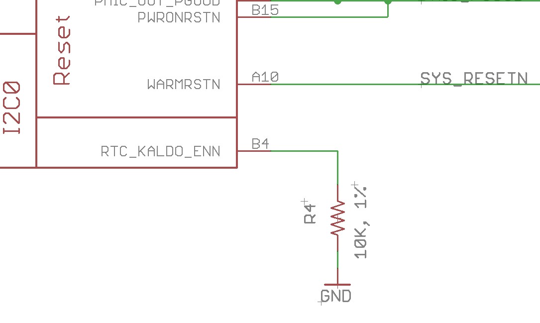
The AM335x processor inside the OSD335x contains a RTC (Real Time Clock) with the potential to support an RTC-Only mode. However, the OSD335x DOES NOT support RTC-Only mode because it uses the C version of TPS65217 which does not support RTC-Only power mode. Although RTC-Only mode is not available, the RTC can still be enabled and used to keep track of time.
The RTC peripheral has an internal LDO which can supply power to it. CAP_VDD_RTC (the supply pin for the RTC core) gets power from the internal RTC LDO if the RTC_KALDO_ENn (active low) pin is pulled low as shown in Figure 50. If RTC_KALDO_ENn is pulled high, the internal RTC LDO will be disabled and CAP_VDD_RTC will have to be connected to VDD_CORE to power the RTC core externally.
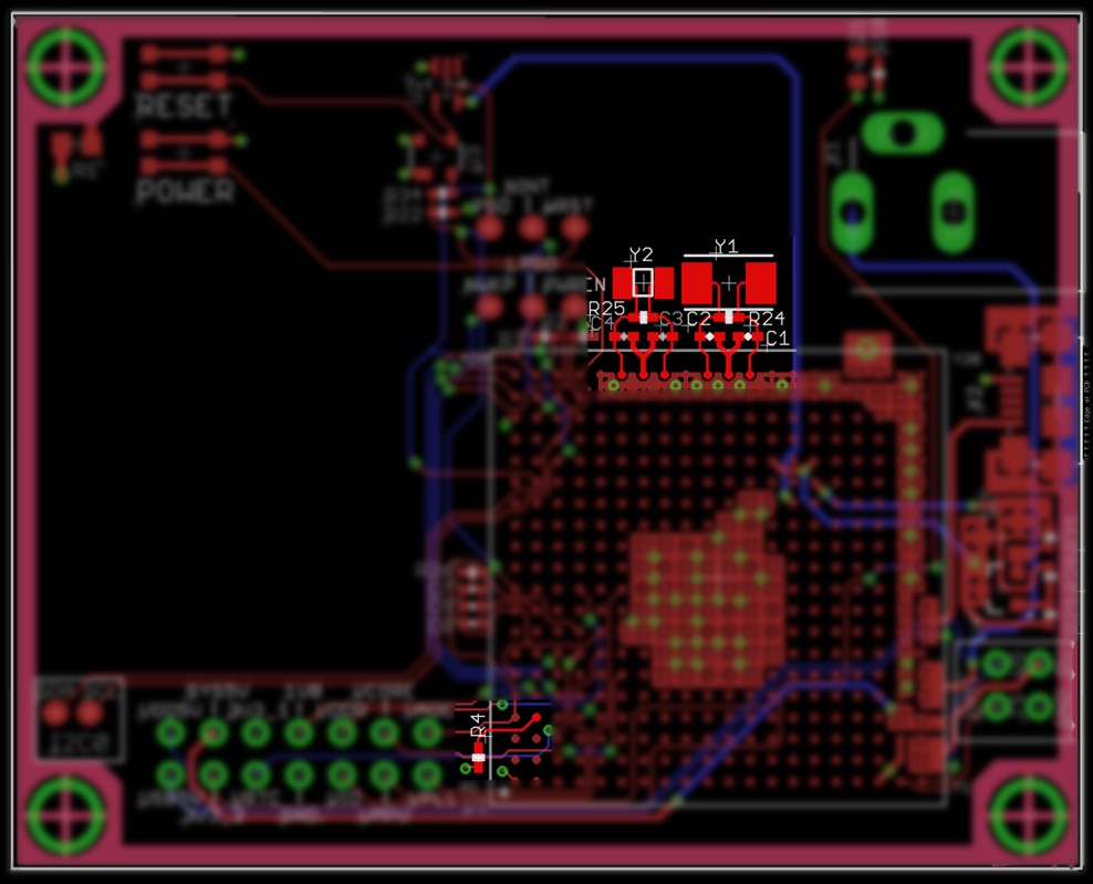
On completion of clock circuitry layout, the board should look like Figure 6 (assuming the board is also populated with power and reset circuitry from previous articles).
| << Return to “OSD335x Reset Circuitry” | Continue to “OSD335x Peripheral Circuitry” >> |
