OSD335x Peripheral Circuitry
Published On: August, 3, 2017 By: Eshtaartha Basu | Updated: July 18, 2018 by Cathleen Wicks
Introduction
Now that the power, reset and clocks are all connected, we need to add the ability to program the OSD335x to make our design useful. To program the OSD335x, we are going to use the JTAG connection to the processor (later lessons will look at other boot devices). To enable us to do some fun things with our design, we will add a couple of general purpose LEDs, switches, and a multipurpose peripheral header. The header will allow us to connect daughter boards to extend functionality.
Prerequisite
This article is a part of the broader OSD335x Reference Design Lesson 1 series which consists of a sequence of articles designed to help you build the bare minimum circuitry required to boot the OSD335x.
We recommend reading the article OSD335x Clock Circuitry before this one. This article builds upon the foundation outlined in it.
All design files for this lesson can be downloaded here.
This article as well as the entire OSD335x Design Tutorial can be downloaded here.
JTAG
For this design, we do not include any non-volatile storage to allow us to boot and run an OS by default. Therefore, all programs will need to be loaded via the JTAG interface.
More information about JTAG interface can be found here.
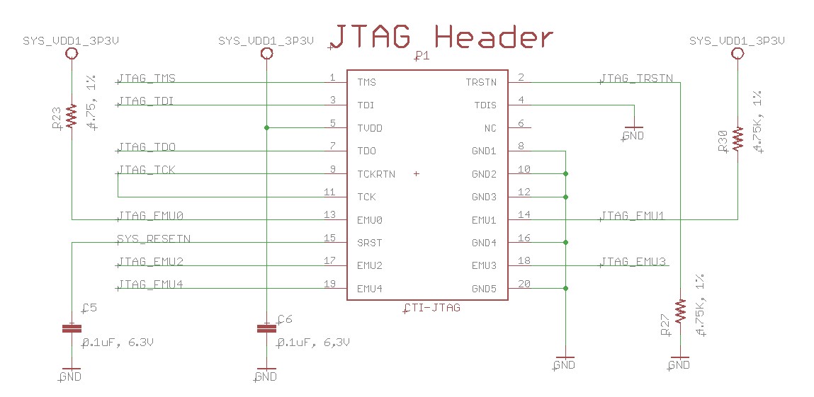
The JTAG circuit can be built on the schematic as shown in Figure 1. This uses a standard 20-pin connector and supports most JTAG debuggers. The JTAG header can be found in the given library under the device name CTI-JTAG.
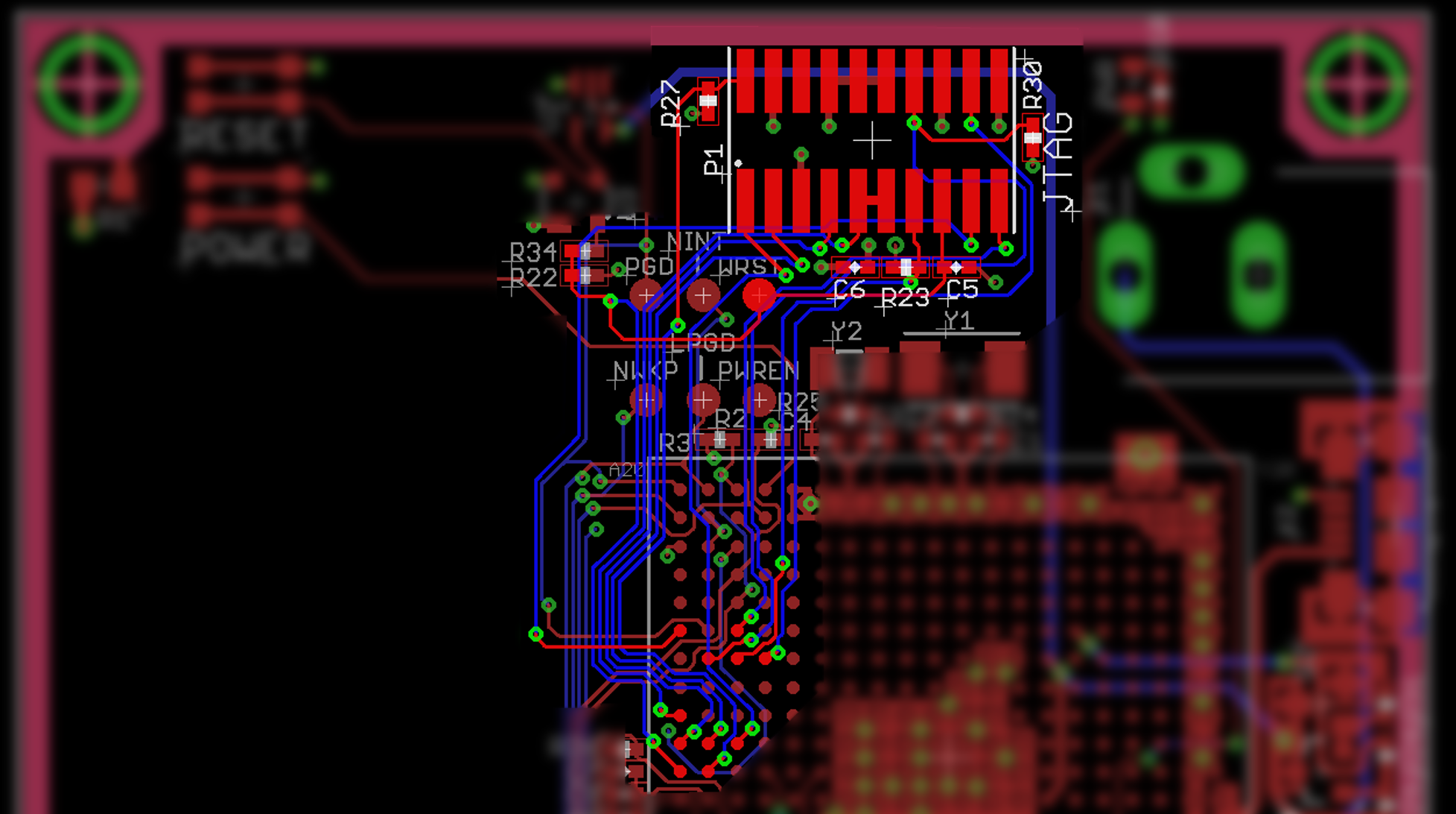
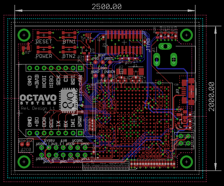
The JTAG connections can be made in the layout as shown in Figure 2.
Boot configuration
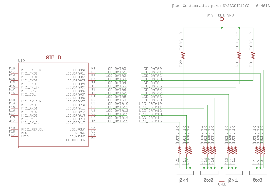
LCD_DATA0 to LCD_DATA15 pins are multiplexed with the SYSBOOT boot configuration pins of the OSD335x. More information about the function of each of these pins can be found in SYSBOOT Configuration Pins section of the AM335x Technical Reference Manual (TRM). SYSBOOT[0] corresponds to LCD_DATA0 while SYSBOOT[15] corresponds to LCD_DATA15.
The state of the boot configuration pins are latched during the rising edge of Power On Reset input, PWRONRSTN.
Using the boot configuration pins for this design, we will:
- Set clock frequency to 24MHz.
- Disable CLKOUT1 output through XDMA_EVENT_INTR0 since this pin will only be used for JTAG emulation.
- Set the boot sequence to SPI0 -> MMC0 -> USB0 -> UART0
By default, if no valid boot images are found during the boot sequence, then JTAG can take control of the processor to allow software to be loaded.
To achieve this, we need to set SYSBOOT[15:0] = 0x4018.

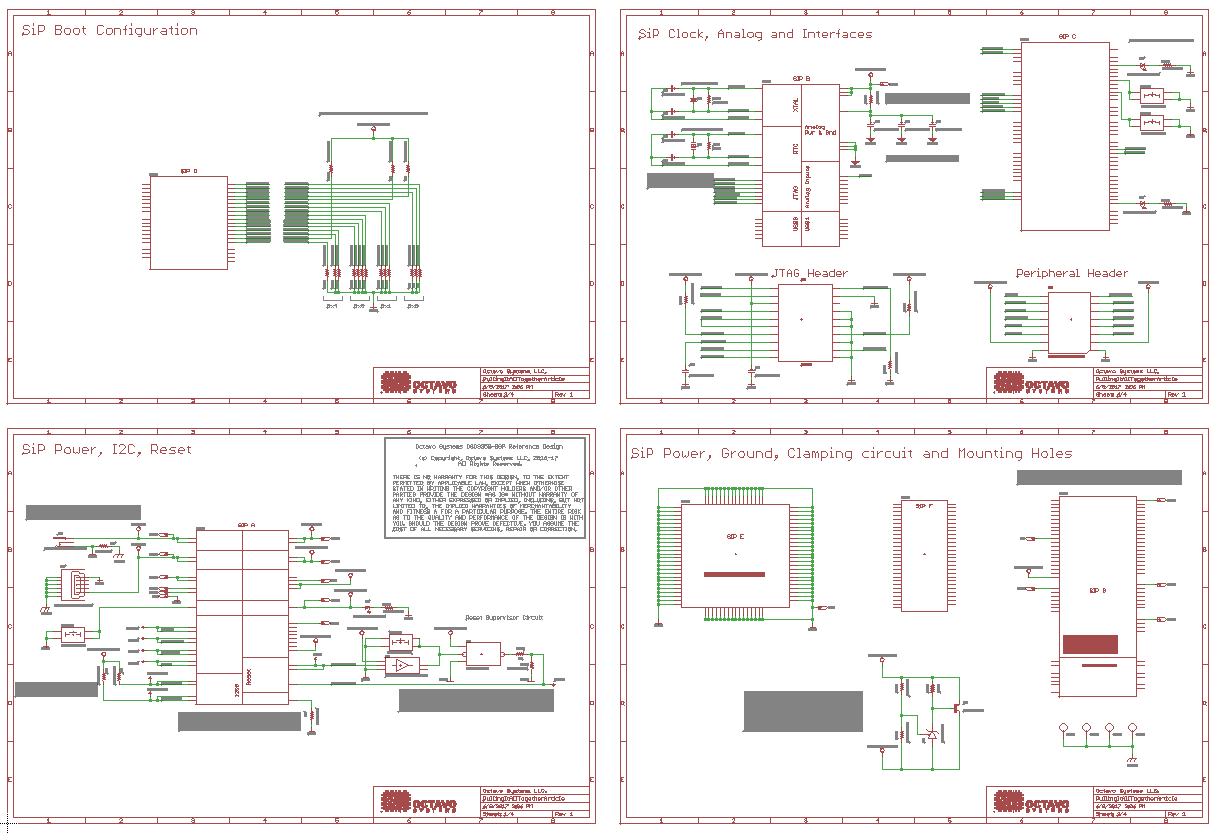
We can build the schematic for the boot configuration as shown in Figure 3.
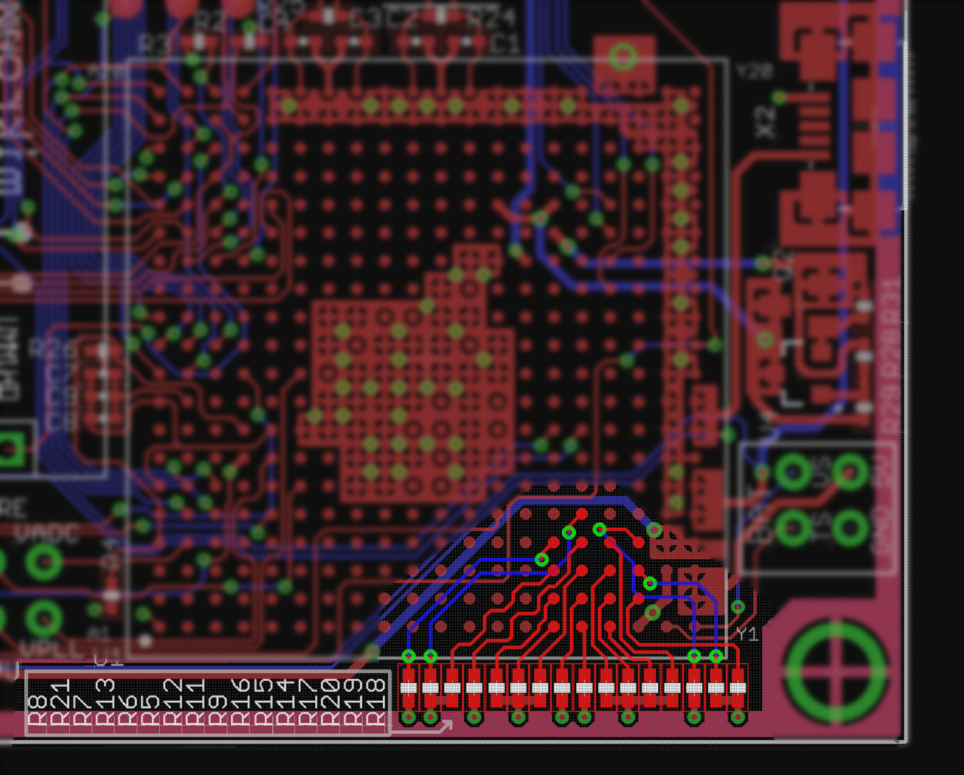
The boot configuration connections in the layout are highlighted in Figure 4.
Buttons and LEDs
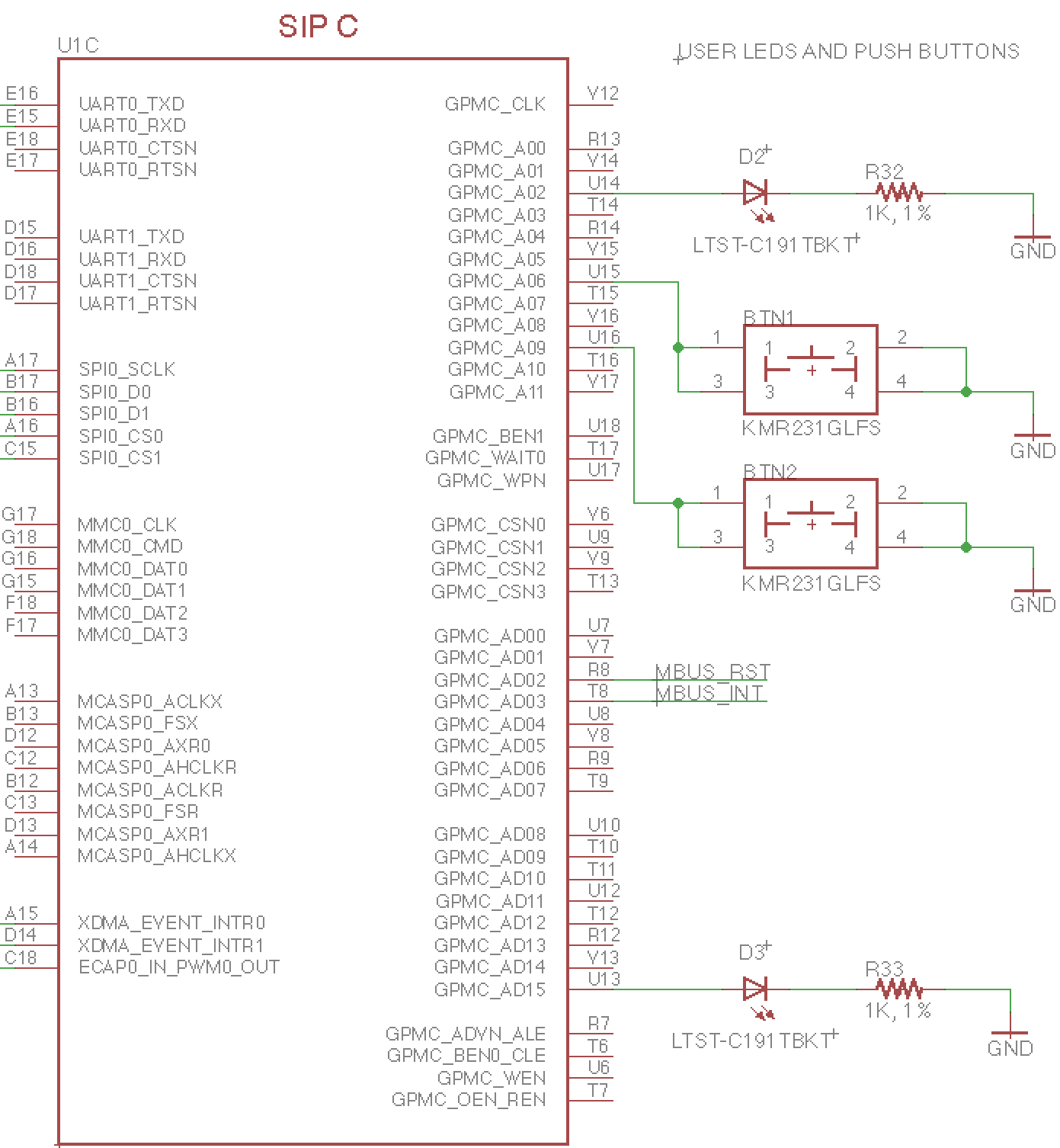
For this design, we will add two push buttons and two LEDs. The buttons can be connected to GPIOs GPMC_A06 and GPMC_A09. These two pins were chosen to make routing easier. There was no de-bounce circuitry added to the buttons so any de-bouncing must be done in software.
Also, let’s add two LEDs, one to GPIO GPMC_A02 and the other to a PWM capable GPIO GPMC_AD15 so that we can exploit the PWM capability of the OSD335x. The schematic for these connections is shown in Figure 5.
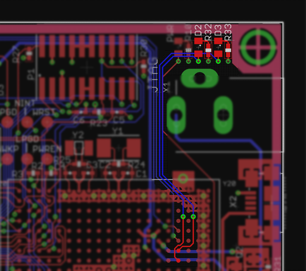
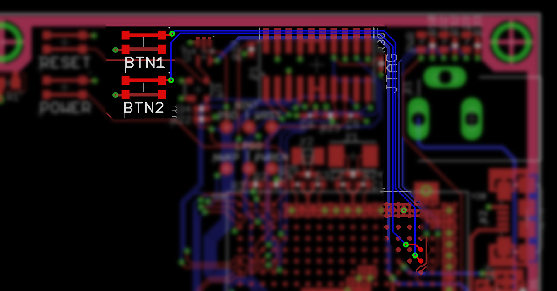
The layout connections for user LEDs and user buttons can be made as shown in Figure 6 and Figure 7.
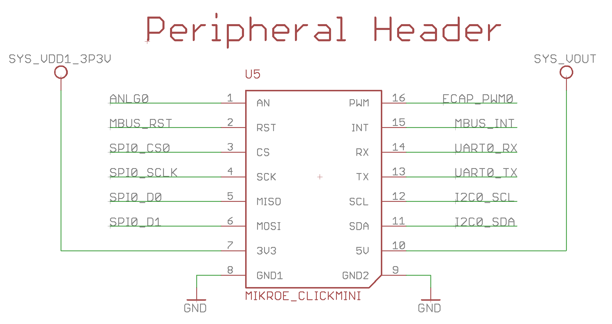
Peripheral header
The OSD335x supports several serial communication protocols like UART, SPI and I2C. These protocols can be used to communicate with and control external devices.
We can map these signals to a standard peripheral header to provide expandability and additional functionality.
The peripheral header we’re using consists of a pair of 1×8 female headers with pin configuration as shown in Figure 8. In the given library, the peripheral header can be found under the device name MIKROE_CLICKMINI (MIKROE_CLICK). This configuration is compatible with mikroBus® Click Board™. Click Boards are daughter boards with a single IC, module or circuit that brings specific functionality to a target main board. Hundreds of click boards are available with various types of sensors, transceivers and functionality.
More description about mikroBus socket and Click boards can be found at:
https://www.mikroe.com/mikrobus/
You can browse through available click boards at:
https://shop.mikroe.com/click.
The peripheral header schematic is given below:
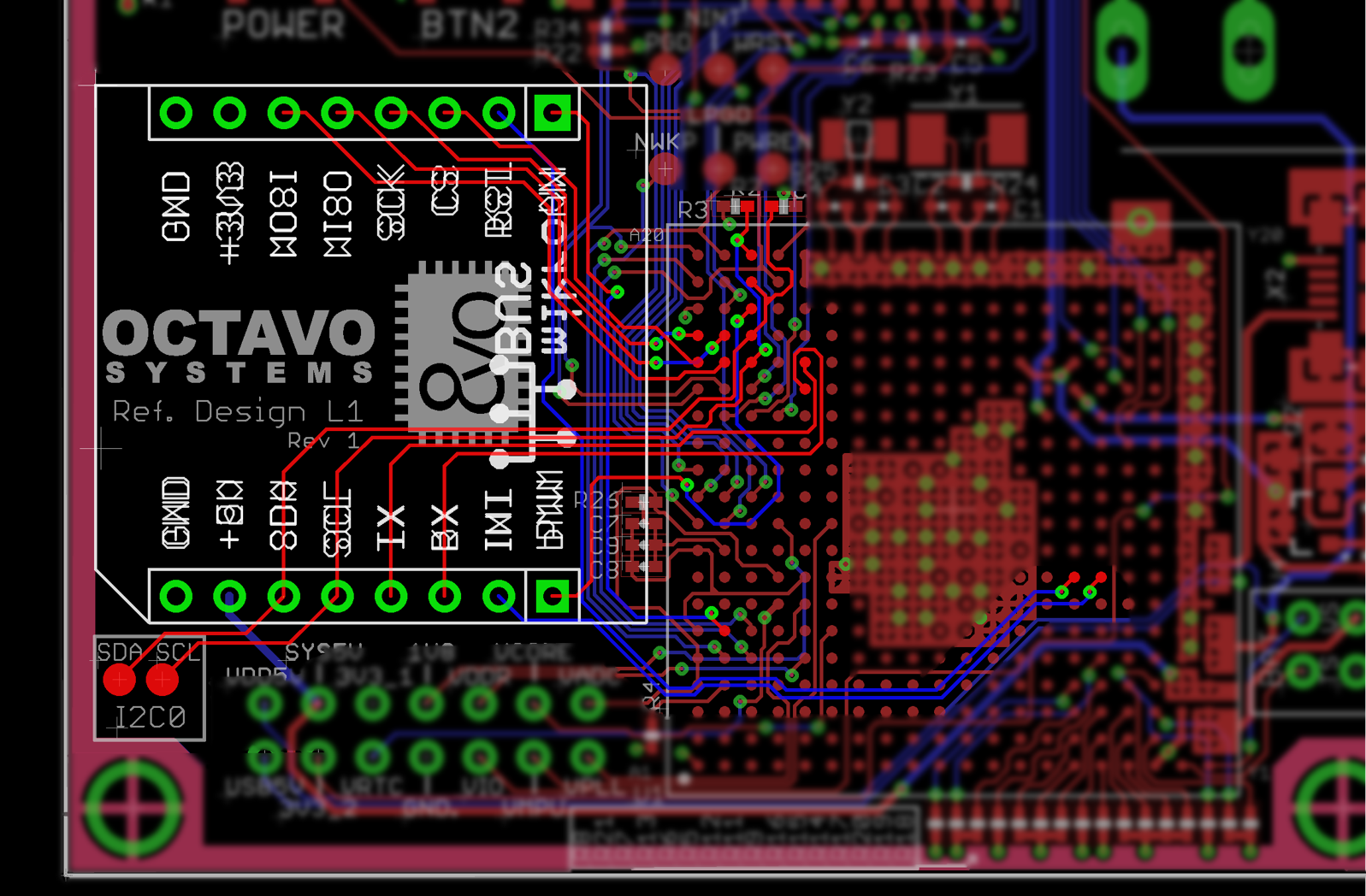
The footprint for peripheral header is shown in Figure 9 and the connections are highlighted.
Finalizing the silkscreen
Silkscreen on a PCB is used to identify components, test points, warning symbols, certification symbols, company logos, PCB name and revision, and any other text that is necessary to document the functionality of the board. During the placement and routing phases of the board design, you should not really worry about the silkscreen. However, now that we have completed placement and routing of all the components on the PCB, we need to make sure that the silkscreen is readable. We need to make sure:
- All the component designators are placed appropriately next to their corresponding components.
- Pin 1 is marked for necessary components. This includes all ICs, connectors and polarized capacitors.
- There is no silkscreen over any component pads. This can lead to bad solder joints.
- The font size of the component designators is as large as possible given the space constraints of the board so that the text is readable.
- Try to not place silkscreen over vias. Silkscreen has a hard time adhering to the annular ring of a via which can make the text difficult to read.
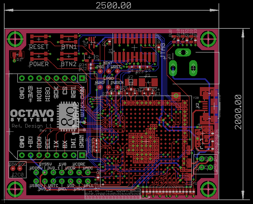
When designing a board, the actual size of the text can be deceiving since the view in the design tool is generally many times larger than the actual board. The minimum font size you should use is 24mils with 8% ratio. Depending on your eyes, a font size of 32mils with an 8% ratio is readable without magnification. This is a good size for passive designators, though in general bigger is better. You can also increase the ratio of the text to make the line width thicker. This can help make the text more readable but only up to a point. However, once you get larger fonts (over 50mils), you should use larger ratios (12% or greater) to make the text more readable. It is recommended that once you are done with updating the silkscreen, print out the silkscreen layers to check their readability.
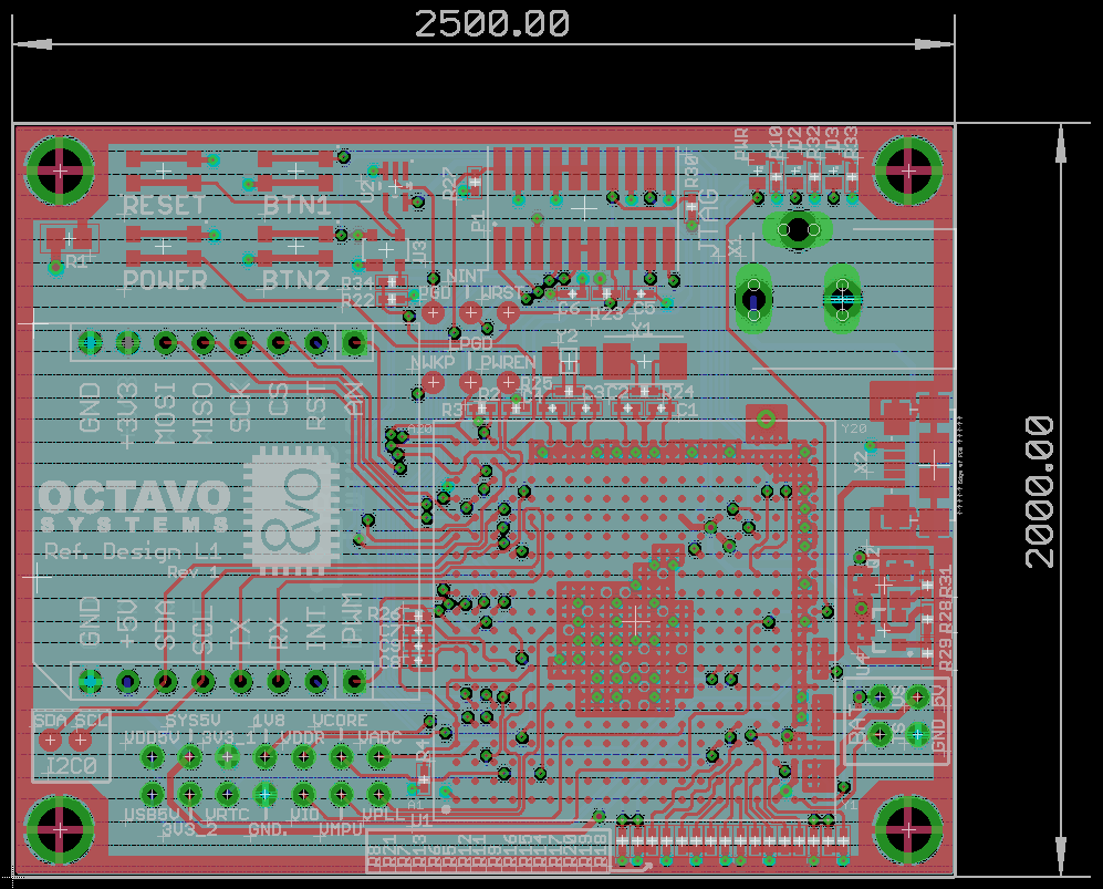
You can also import a picture of your logo into Eagle and add it into your layout. You can learn more about the procedure to import images here. For our design, we have added Octavo Systems logo along with the lesson name and revision number as shown in Figure 11, Figure 12 and Figure 13.
Expected outcome
Now that we have completed building the schematic and layout, the complete schematic should look similar to Figure 10 and complete layout should look similar to Figure 11, Figure 12 and Figure 13.
PCB order process
The PCB order process begins with Bill Of Material (BOM) generation. EAGLE is capable of maintaining manufacturer and part number for each component so the schematic can be the controlled document for manufacturing information. The BOM.ulp can be used to output this data in an easily readable format. Once BOM is generated, the components can be purchased.
The next step is gerber file generation for PCB manufacturing. More information on gerber file generation, gerber verification and order placement can be found here.
| << Return to “OSD335x Clock Circuitry” | Continue to “OSD335x Board Bring Up and Demo” >> |
