OSD335x Lesson 2: USB Circuitry
Published On: April, 20, 2018 By: Eshtaartha Basu | Updated: July 31, 2018 by Cathleen Wicks
1 USB Circuitry
1.1 Introduction
The Universal Serial Bus (USB) is an industry standard that was introduced in 1996 to standardize the connection between computer peripherals. USB interfaces are used to exchange data and power between two or more devices. USB has been successful in replacing several older and slower interfaces like serial ports and parallel ports.
The OSD335x has two independent identical USB 2.0 peripherals (USB0 and USB1). Each peripheral supports USB Host, Peripheral (Client), and On-The-Go (OTG) modes with a line/bus speed of up to 480Mbps.
This article will give you necessary information about the different USB pins, how to put the USB peripherals of the OSD335x into the different USB modes, schematic/layout methodology and USB Testing for OSD335x.
Prerequisite
This article is a part of the broader OSD335x Reference Design Lesson 2 series which consists of a sequence of articles designed to help you build the bare minimum circuitry required to boot Linux on the OSD335x. We recommend reading the article OSD335x Lesson 2:Introduction to Bare Minimum Circuitry for Linux Boot before this one. This article builds upon the foundation outlined in it.
All design files for this lesson can be downloaded here.
Table of Contents
1USB Circuitry
1.1Introduction
1.2USB Pins
1.3USB Modes and their Configuration on the OSD335x
1.3.1USB Host Mode
1.3.2.USB Peripheral (Client) Mode
1.3.3USB OTG Mode
1.4USB Schematics
1.5USB Layout
1.6USB Testing
![]()
![]() A PDF version of this Lesson as well as the entire OSD335x Design Tutorial can be downloaded here.
A PDF version of this Lesson as well as the entire OSD335x Design Tutorial can be downloaded here.

1.2 USB Pins
USB 2.0 connectors have either 4 or 5 pins, depending on the form factor / USB mode. These pins are:
| Pin | Type | Description |
|---|---|---|
| VBUS | Power | 5V power rail |
| DM (or D-) | I/O | USB Data Differential Pair |
| DP (or D+) | I/O | |
| ID | I | USB Mode Control Pin (not present on 4 pin connectors) |
| GND | Power | Ground |
A USB 2.0 Host connector has 4 pins (ID is assumed to be grounded) and can provide up to 500 mA of current at 5V. A USB 2.0 Peripheral (Client) port has 4 pins (ID is assumed to be high) and can source up to 500mA of current at 5V. A USB 2.0 OTG port requires 5 pins. This allows the port to be dynamically configured to be either a Host or a Peripheral (Client) by setting the ID pin voltage level.
When configured as a Host port, the USB controller will act as a master and send data and commands to the attached slaves. When configured as a Peripheral (Client) port, the USB controller will act as a slave and respond to data and commands sent to it by the master (Host).
The USB peripherals of the OSD335x contain the physical interface circuitry (PHY) to allow them to talk directly to other USB devices and each can be configured independently as either a Host or a Client. To support this configurability, each USB peripheral has seven pins which are listed in Table 2
| Pin | Type | Description |
|---|---|---|
| USBx_DP | I/O | USBx Data Differential Pair |
| USBx_DM | I/O | |
| USBx_DRVVBUS | O | USBx external power logic control |
| USBx_VBUS | I | USBx external power logic voltage sense |
| USB_ID | I | USBx Mode Control Pin |
| USB_CE | O | USBx Charge Enable |
- USBx_DP/DM: These are differential I/O pins that carry data.
- USBx_DRVVBUS: The USB peripherals themselves cannot supply the necessary current to support Host mode. Therefore, the USBx_DRVVBUS output pin was provided to control external 5V power logic used to supply power to a Host port.
- USBx_VBUS: This input pin is used to sense the voltage of the VBUS pin . For the USB peripheral to be enabled, a valid voltage (>=4.4V) should be placed on this pin.
- USB_ID: The mode of USB peripheral depends on the state of this pin.
- USB_CE: Each USB PHY contains circuitry that can automatically detect the presence of charger on the USB port. If a charger is detected, this pin goes high and remains high until the charger is disabled through software. For more information, please refer USB Charger Detect section of AM335x TRM (Section 9.2.4.4.2 of SPRUH73P). In general, this pin is not used.
1.3 USB Modes and their Configuration on the OSD335x
The three different USB modes supported by the USB peripherals of the OSD335x are described in this section.
1.3.1 USB Host Mode
In Host mode, the USB port will be able to supply power, control and communicate with all the connected Client devices. For example, the USB ports on most desktop computers and laptops operate in Host mode.
The USB peripherals of the OSD335x can be configured in Host mode in 2 ways:
Hardware Method: Ground the USBx_ID pin and use an appropriate USB A type connector on the cable end.
Software Method: Program the firmware to set the respective USBxMODE register IDDIG bit to 0.
Once the USB controller determines its role is a Host, it will drive USBx_DRVVBUS pin high to enable external 5V power logic and wait for USBx_VBUS input pin to go high. If USBx_VBUS does not go high (>=4.4V) within the next 100ms, it will generate a VBUS error interrupt that can be handled by software. However, if a valid voltage is found on USBx_VBUS, the controller will wait for a Client device to connect.
1.3.2 USB Peripheral (Client) Mode
In Client mode, the USB device receives power from the Host and the device can only communicate with the Host. The USB peripherals can be configured in Peripheral (Client) mode in 2 ways:
Hardware Method: Leave the USBx_ID pin floating and use an appropriate USB B type connector on the cable end.
Software Method: Program the firmware to set the respective USBxMODE register IDDIG bit to 1.
The USB controller will begin operating in Peripheral (Client) mode only if it detects a valid voltage (>=4.4V) on USBx_VBUS input.
1.3.3 USB OTG Mode
On-The-Go (OTG) mode allows the USB port to dynamically switch between Host and Peripheral (client) mode based on requirement in space constrained applications like tablets or smartphones.
The USB peripherals in OTG mode assume the role of Host or Peripheral (Client) based on the status of ID pin which is directly controlled by the USB cable.
The configuration of the USB peripherals for different modes in summarized in Table 3.
| Configuration | |||
|---|---|---|---|
| Through Hardware | OR | Through Software* | |
| USB Host | Ground USBx_ID | Set IDDIG bit of USBxMODE register to 0 | |
| USB Client | Leave USBx_ID floating | Set IDDIG bit of USBxMODE register to 1 | |
| USB OTG | USBx_ID is directly controlled by USB Cable Connector | Set IDDIG bit to either 0 or 1 based on mode requirement | |
* If the USBx mode is being controlled purely through software, you may have to suitable manage other registers also along with IDDIG pin. For more information, refer USB Controller Host and Peripheral Modes Operation section of AM335x TRM.
1.4 USB Schematics
In this section, we will build schematics for to configure the USB1 peripheral in Host mode and the USB0 peripheral in OTG mode.
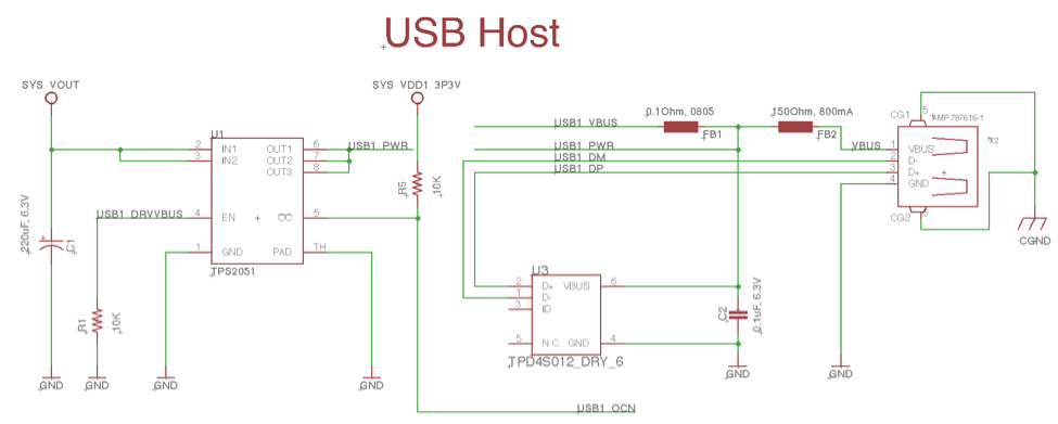
Let’s begin with the USB1 as a Host port. As described in the previous section, a USB Host port is required to supply power to its clients. Hence, we will need an external 5V power switch to supply the appropriate amount of power. The OSD335x will use the USB1_DRVVBUS output to enable/disable the power switch and will use the USB1_VBUS input to sense the presence of required output voltage. Given that there is generally a lot of interaction with the USB port, it is important to add electro-static discharge (ESD) protection to the signals going to the processor. Therefore, a 4-channel ESD Protection chip has also been added to the circuit.
For this lesson, we will be using be using a TPS2041 external power switch, a TPD4S012 4-channel ESD Solution, and an AMP 787616-1 USB A Female Connector. You may use different components in your design based on your requirements.
In order to isolate the power supplied by the board from any external noise on the USB VBUS line, a Ferrite bead is placed between the output of the power switch and the connector. Similarly, in order to isolate the USB1_VBUS input from any power supply noise on the board, a Ferrite bead will be placed between the output of the power switch and the USB1_VBUS input.
The symbols for the TPS2041, TPD4S012, AMP 787616-1 and Ferrite beads are available in the provided library. The USB Host circuit can be built as shown in Figure 1.
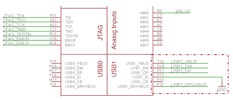
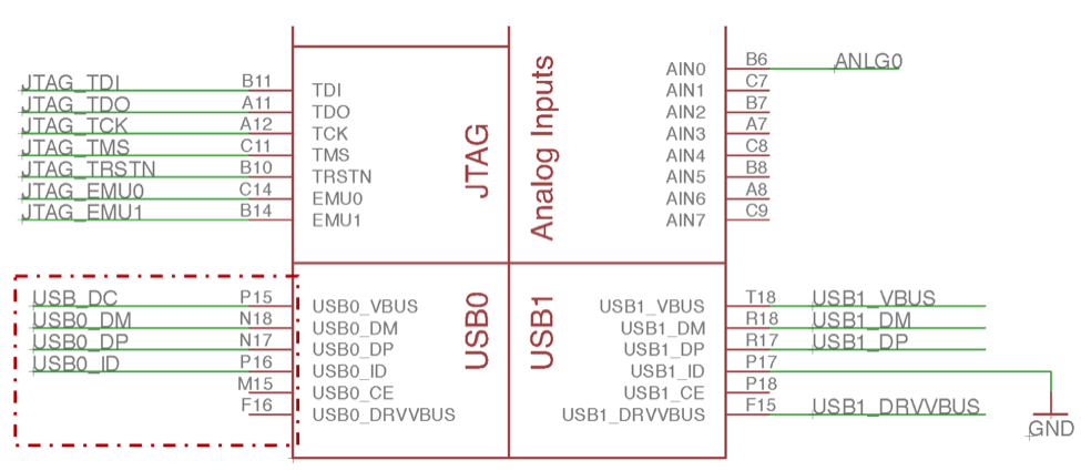
The USB1 signal connections to the OSD335x are shown in Figure 2 (The changes made are highlighted in the dotted lines).
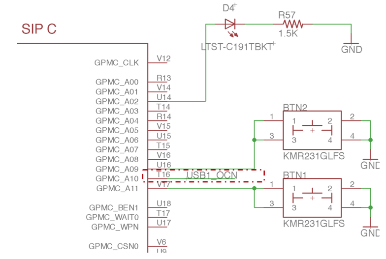
The active low Over Current output of the Power Switch (pin 5 of the TPS2501 attached to the USB1_OCN signal in Figure 1) can be connected to any of the GPIOs of the OSD335x as shown in Figure 3 (GPMC_A10 pin is chosen in this case) to detect issues with USB Client devices trying to draw more power than allowed.
Now, let’s configure USB0 as a USB Client (technically we will configure this as an OTG port since we will connect the ID pin, but primarily this port will be used as a client. To use this as a Host port, power will need to be applied externally to the USB5V test point.). A USB Client can receive power from its host using the VBUS line of the USB client connector. The OSD335x can source power from multiple input sources, including 5 volts from a USB connector. Therefore, to provide flexibility when powering this board, we can connect the VBUS line of the USB client connector to the USB Power Input pins of the OSD335x, i.e., VIN_USB. Similar to the USB Host connections, we also have to connect the VBUS input to the USB voltage sense input of the OSD335x, USB0_VBUS, and add a TPS2041 ESD protection chip.
The symbol for USB Client Connector (10118192-0001LF) is available in the provided library. The USB Client circuit is shown in Figure 4. This USB Client connector is the same connector used in Lesson 1 for the USB Input Power. Now, we have to connect the USB signals and ESD protection chip.
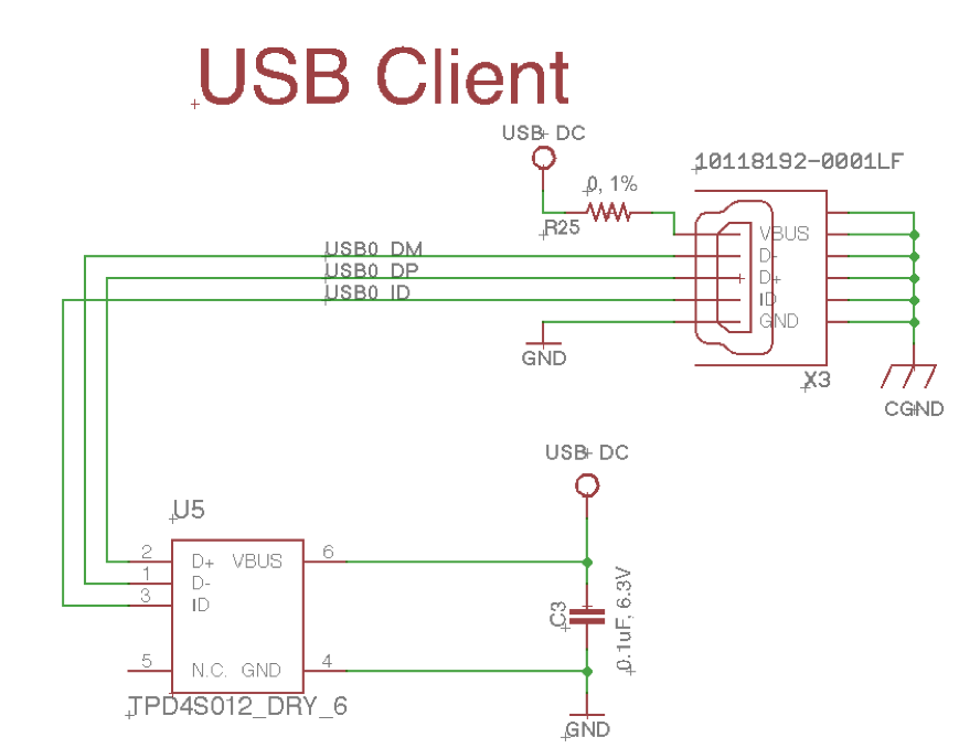
The USB0 signal connections to the OSD335x are shown in Figure 5 (The changes made are highlighted in the dotted lines).
1.5 USB Layout
USB lines operate at very high speeds (up to 480Mbps) and use differential signaling. Therefore, we need to follow certain guidelines to ensure good layout and proper operation.
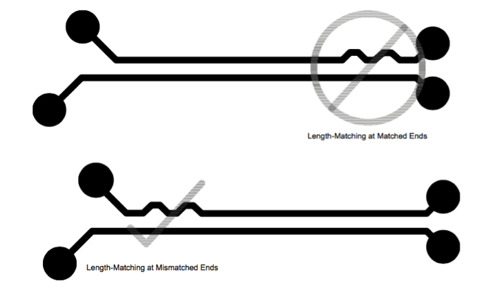
- Length matching the differential pair (D+ and D-) is critical in USB layout design. The thumb rule is to maintain the length difference < 1%.
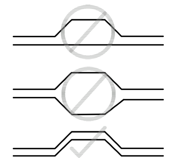
- If the trace lengths are mismatched, try to match them at the mismatched end and not on the matched end using serpentine traces. When using serpentine traces, the please be careful that the width between the bends is greater than 3x the trace width and that all angles are at least 135 degrees. An example for this is shown in Figure 6
- Route the differential pair symmetrically and parallel to each other.
- It is best to route the differential pair over a solid Ground plane. Avoiding routing over split planes or plane voids.
- When through-hole USB connectors are used, it is better to route the differential pair on the bottom layer instead of top layer so that the connector pins can be directly reached on the bottom layer. This prevents the connector pins from acting as stubs.
- Try to avoid routing differential pair near clock signals or any other signals that may cause interference.
- The D+ to D- impedance must be 90 Ohms and the impedance of either line to ground must be 30 Ohms. This is straight forward to do on a 4 layer PCB. However, you can route USB on a two layer PCB. See http://www.focusembedded.com/blog/high-speed-usb-in-a-two-layer-pcb/ for a discussion on additional considerations to accomplish this.
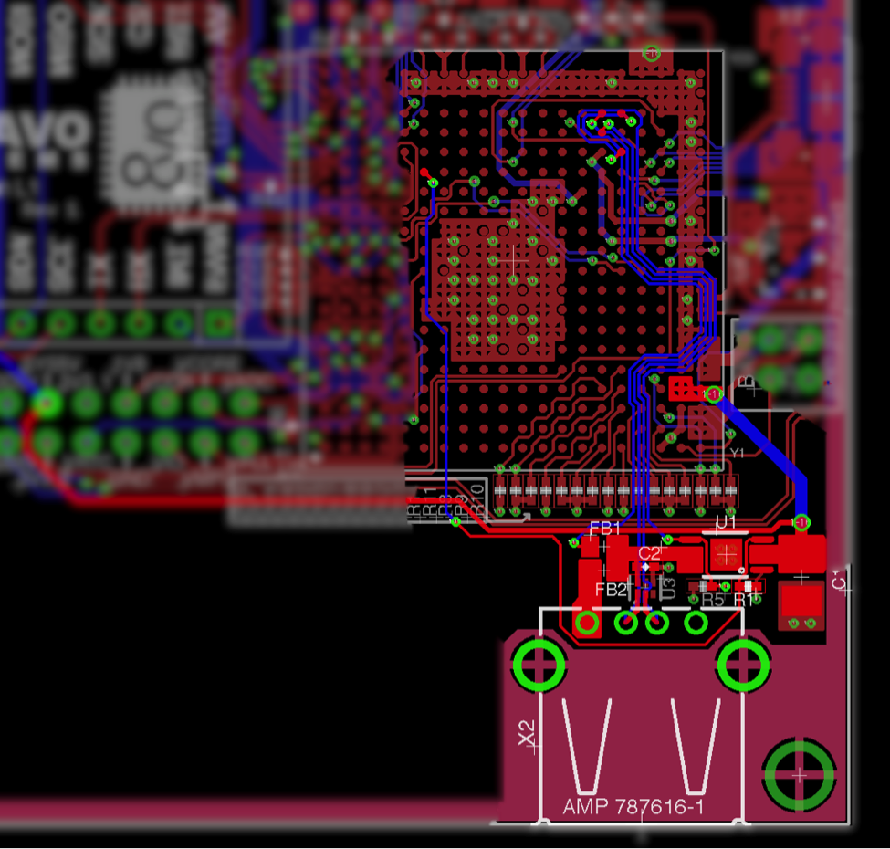
Keeping the above guidelines in mind, the USB Host and Client circuitry can be laid out as shown in Figure 8 and Figure 9 respectively.

1.6 USB Testing
Testing the integrity of USB signal is very important since it operates at high speed. An eye diagram is commonly used for this purpose. The eye diagram test will measure the rise time, fall time, undershoot, overshoot and jitter of USB signal. You can put the official USB compliance logo on your device only after your device passes the appropriate tests. More information about USB compliance tests and procedure can be found here.
*****
| << Return to “OSD335x Lesson 2 Introduction to Bare Minimum Circuitry for Linux Boot” | Continue to “OSD335x Lesson 2 Adding Non-Volatile Storage” >> |
