OSD335x Lesson 2: Adding Non-Volatile Storage
Published On: May, 1, 2018 By: Eshtaartha Basu | Updated: January 13, 2021 by Greg Sheridan
1 Adding Non-Volatile Storage
1.1 Introduction
In order to store programs, files, and data so that Linux can boot easily and retain information across power downs, non-volatile storage needs to be attached to the OSD335x. This can be done using floating gate non-volatile memories such as embedded Multi-Media Card (eMMC), Secure Digital (SD) Card, or electrically erasable programmable read-only memory (EEPROM). The floating gates are used to store information in the form of 0s and 1s and can retain data when power is removed from the device.
The main differences between an eMMC or an SD Card and EEPROM are speed, data density and longevity. EEPROM is typically byte addressable with limited read/write cycles and has a lower data density. It also operates relatively slowly but has a much lower cost when a small amount of non-volatile storage is required. Whereas, in an eMMC or an SD Card (also known as Flash memory devices), data is read and written in large blocks or pages which helps it operates faster. Since flash memory devices are not byte addressable, all the circuitry required for byte addressability is removed and hence they can pack a higher data density. Additionally, eMMC has circuitry that increases robustness against data corruption due to power down events. Hence, in embedded applications, eMMCs and SD Cards are generally used to store the Linux OS, filesystem, applications and related data whereas EEPROM is generally used to store board or device identification (ID) and hardware configuration information.
The OSD335x has three MMC/SD Controllers that can interface with flash memory devices like an eMMC or an SD Card. For our board, we will use MMC0 to interface with a microSD Card connector and MMC1 to interface with an eMMC device.
The OSD335x also has many I2C peripherals that can be used to interface with the EEPROM. For our board, we will use the I2C0 peripheral to interface with the EEPROM. The OSD335x has to use an external EEPROM for the board and device ID. However, the OSD335x-SM integrates an EEPROM within the package. Within the OSD335x-SM, the EEPROM is also connected on I2C0.
This article will help you connect an eMMC, SD card and EEPROM to the OSD335x by giving you necessary information about their corresponding circuits, schematic and layout. We will also be discussing the steps needed to finalize the Lesson 2 PCB design and sending it for manufacturing.
Prerequisite
This article is a part of the broader OSD335x Reference Design Lesson 2 series which consists of a sequence of articles designed to help you build the bare minimum circuitry required to boot Linux on the OSD335x. We recommend reading the article OSD335x Lesson 2: USB Circuitry before this one. This article builds upon the foundation outlined in it.
All design files for this lesson can be downloaded here.
Table of Contents
1Adding Non-Volatile Storage
1.1Introduction
1.2MMC/SD Circuitry
1.2.1SD Card
1.2.2eMMC
1.3.EEPROM Circuitry
![]()
![]() A PDF version of this Lesson as well as the entire OSD335x Design Tutorial can be downloaded here.
A PDF version of this Lesson as well as the entire OSD335x Design Tutorial can be downloaded here.

1.2 MMC/SD Circuitry
Each MMC/SD instance of the OSD335x has several pins. The name and function of the important pins are listed in Table 1.
| Pin | Type | Description |
|---|---|---|
| MMCx_CLK | I/O | MMC/SD serial clock output |
| MMCx_CMD | I/O | MMC/SD command signal |
| MMCx_DAT [7:0] | I/O | MMC/SD data signals |
| MMCx_SDCD | I | SD card detect (from connector) |
- MMCx_CLK: This pin provides the clock to a MMC or SD device from the MMC/SD controller.
- MMCx_CMD: This pin is used for two-way communication between the connected MMC or SD device and the MMC/SD controller. The MMC/SD controller transmits commands to the device and the device drives responses to the commands on this pin.
- MMCx_DAT [7:0]: Depending on the device you are using, you may need to connect 1, 4, or 8 data lines. The number of DAT pins (the data bus width) is set by the Data Transfer Width (DTW) bit in the MMC control register (SD_HCTL) and DW8 bit in SD_CON register. For more information, see MULTIMEDIA_CARD Registers section of AM335x TRM.
- MMCx_SDCD: This input pin serves as the SD card detect. This signal is generated by a mechanical switch on an SD card connector.
1.2.1 SD Card
The Device Tree of the Linux image you will be using expects an SD card on MMC0 and an eMMC on MMC1 interface of the OSD335x. Therefore, we will use MMC0 for our SD card circuit. The SD card circuit can be built around MMC0 as shown in Figure 1 and Figure 2. According to JEDEC Standard No. 84-A43 which is the eMMC standard implemented by the AM335x processor inside the OSD335x, MMC DAT and CMD lines have to be pulled up to prevent them from floating when no card is inserted.


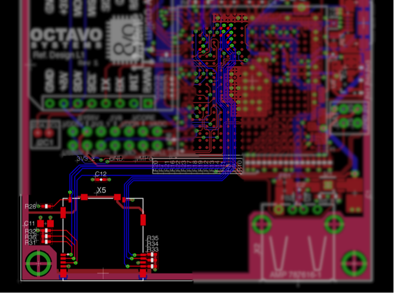
The SD card layout can be made as shown in Figure 3. The MMC bus operates at a moderately high speed. Therefore, you should try to keep all of the traces of the bus about the same length.
1.2.2 eMMC
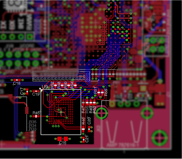
Similar to the SD Card circuit, the eMMC circuit can be built around MMC1 as shown in Figure 4 and Figure 5. The RST# input of the eMMC can be controlled by any of the GPIOs of the OSD335x (we used the GPMC_A04 pin for this design).
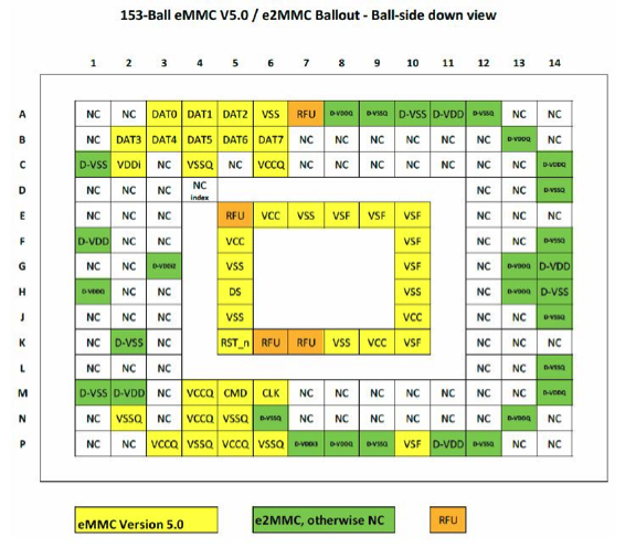
For this lesson, we’ll be using Kingston 153 (HS200) 16GB eMMC. Its symbol and footprint are available in the given library. However, it can be difficult to source eMMC memory. As long as the memory follows the 153 ball JEDEC eMMC standard, it can be used in this lesson.


The eMMC traces can be laid out as shown in Figure 6. Similar to the SD card layout, you should try to keep all of the traces of the bus about the same length.
.
1.3 EEPROM Circuitry
During boot, the U-boot bootloader of the Linux image you will be using read an on-board EEPROM for a board ID. This allows U-boot to configure the pins and set other appropriate boot environment variables. By default, the Linux kernel will not boot unless a valid board ID is found. However, this check can be bypassed in order to bring up a board or to perform the initial programming of the EEPROM. Given that we will be using a Linux image for this lesson, we need to have an EEPROM connected to I2C0 that is programmed with the appropriate information. More information about loading data to the EEPROM or bypassing EEPROM board ID check can be found on our forum posts #4733 and #4608.
The EEPROM circuit can be built as shown in Figure 8. By default, the Write Protect (WP) pin is pulled high through a 10K Ohm resistor. This means that the EEPROM is write protected and no data can be written to the EEPROM. In order to program the EEPROM, we need to provide test points such that it is easy to connect the Write Protect (WP) pin to a GND pin.

EEPROM layout can be made as shown in Figure 9.

*****
| << Return to “OSD335x Lesson 2 USB Circuitry” | Continue to “OSD335x Lesson 2 Bringing Up a Custom Bare-Bones Linux PCB” >> |
