OSD335x Clamping Circuit
Published On: August, 1, 2017 By: Eshtaartha Basu | Updated: July 18, 2018 by Cathleen Wicks
Introduction
This article is the fourth part of the OSD335x Reference Design Lesson 1 Power circuitry discussion. It will focus on a clamping circuit which may be needed by your application. A clamping circuit is a type of circuit that maintains the voltage level of an input with respect to another input. As we discuss the clamping circuit, we will build the schematic and layout the corresponding traces.
Prerequisite
This article is a part of the broader OSD335x Reference Design Lesson 1 series which consists of a sequence of articles designed to help you build the bare minimum circuitry required to boot the OSD335x.
We recommend reading the third part of power circuitry article OSD335x Power Management before this one. This article builds upon the foundation outlined in it.
All design files for this lesson can be downloaded here.
This articles as well as the entire OSD335x Design Tutorial can be downloaded here.
AM335x Power-Down Requirements
The AM335x datasheet requires that the voltage difference between the power rails VDDS (1.8V) and VDDSHVx [1-6] (3.3V) of the AM335x processor be less than 2V during the entire power-down sequence. More information about this can be found under Use of a Clamping Circuit for Simultaneous Ramp Down section of this user guide. The VDDS power input of the AM335x processor is connected within the OSD335x to the SYS_RTC_1P8V power rail and the VDDSHVx [1-6] power inputs are connected within the OSD335x to the VDDSHV_3P3V power rail. The voltage difference between these two power rails may exceed 2V if VDDSHV_3P3V rail remains high possibly because of large output capacitance or no load being present on the output while, the SYS_RTC_1P8V rail ramps down quickly as if it were fully loaded.
If you cannot guarantee that the voltage difference between the two voltage rails (SYS_RTC_1P8V and VDDSHV_3P3V) of the OSD335x will be less than 2V during the entire power down sequence in your design, then you will need a clamping circuit.
Clamping circuit
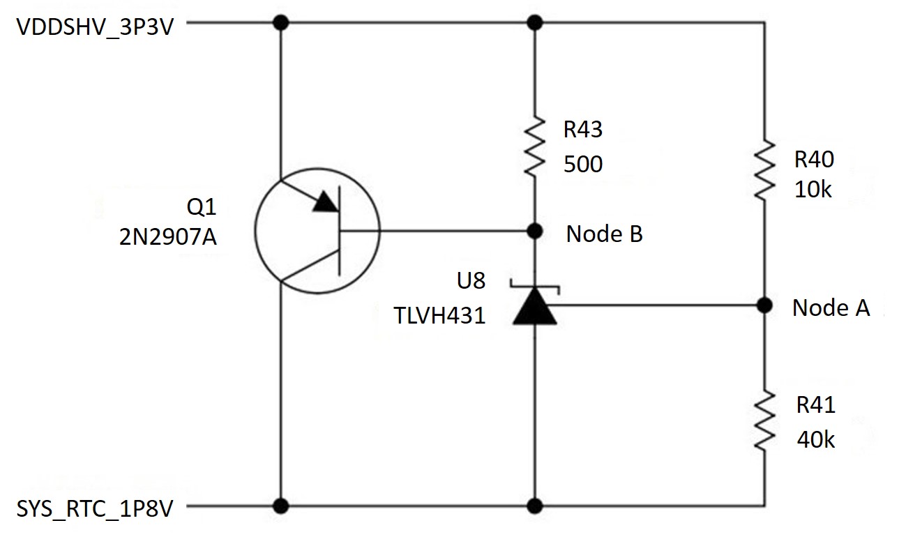
The clamping circuit (shown in Figure 1) will make sure that the voltage difference between the given two voltage rails (VDDSHV_3P3V and SYS_RTC_1P8V) is less than 2V. Its operation will be discussed in three phases.
You need to keep the following assumptions in mind before analyzing the operation of clamping circuit:
- It is assumed that, once the power down sequence of the AM335x begins, the voltage rail VDDSHV_3P3V remains high due to a large output capacitance or no load and the voltage rail SYS_RTC_1P8V ramps down relatively quickly due to a full load.
- It is also assumed that, the voltage rail, VDDSHV_3P3V, will be able to source enough current to pull up the voltage of SYS_RTC_1P8V rail whenever necessary.
We recommend you to read the datasheets of the shunt regulator TLVH431 and 2N2907A transistor before trying to understand the operation of clamping circuit.
Few quick tips about TLVH431 and 2N2907A essential to understand the operation of clamping circuit:
- The shunt regulator, TLVH431, will be OFF (acts as open switch) whenever the voltage at its reference input connected to node A (in Figure 1) is less than 1.24V. It will turn ON (act as closed switch) whenever voltage at its reference input (node A) is greater than 1.24V.
- The PNP transistor, 2N2907A, will allow current to flow from its emitter terminal to the collector terminal when the voltage difference between its base terminal and emitter terminal is greater than or equal to 0.4V. In other words, it acts like a closed switch when the voltage difference between node B and the VDDSHV_3P3V rail is greater than 0.4V and acts like an open switch when the voltage difference between node B and the VDDSHV_3P3V rail is less than 0.4V.
For the circuit analysis below, we will assume that TLVH431 will be in the OFF state whenever the reference input of the TLVH431 is at 1.24V.
Phase 1 – AM335x in normal operation / just before power down (Clamping circuit in standby):
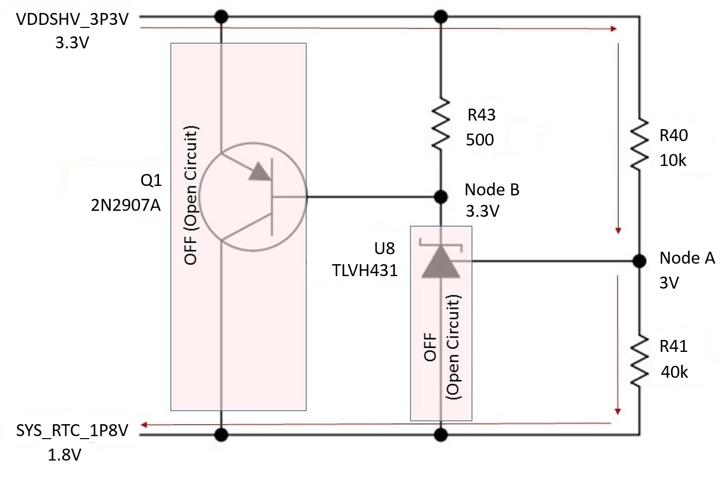
The clamping circuit will operate in this phase when both the voltage rails are at nominal voltages (i.e., VDDSHV_3P3V is at 3.3V and SYS_RTC_1P8V is at 1.8V) as shown in Figure 2.
The voltage divider circuit consisting of resistors R40 and R41 provides the reference voltage for U8 (TLVH431) at node A. In this phase of operation, node A will be at 3V relative to ground. But, node A will be at 1.2V (3V – 1.8V) with respect to SYS_RTC_1P8V voltage rail. As a result, U8 will turn OFF (will not sink current from node B) and voltage at node B will remain at 3.3V. Hence, Q1 (2N2907A) will turn OFF.
Phase 2 – AM335x power down sequence begins (Clamping circuit actively maintaining the voltage difference between the two power rails):
The clamping circuit will operate in this phase when the voltage difference between its two power rails, VDDSHV_3P3V and SYS_RTC_1P8V, is greater than or equal to 1.55V. Let’s discuss the two possible cases:
Case 1: Voltage difference between VDDSHV_3P3V and SYS_RTC_1P8V is equal to 1.55V
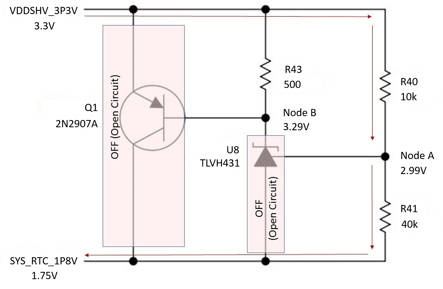
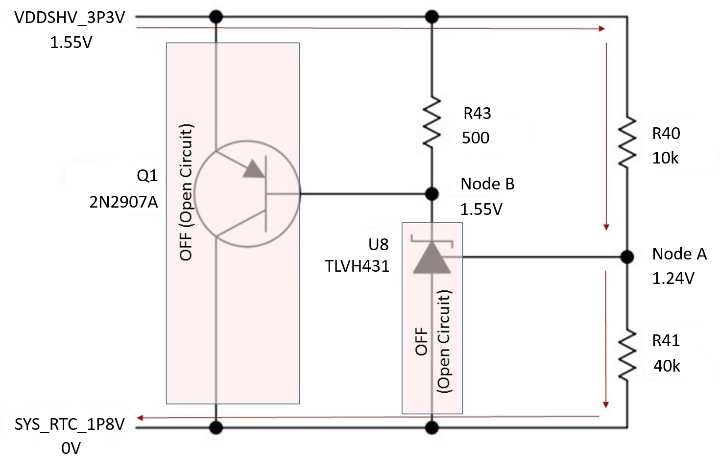
Let’s understand case 1 through an example. For this example, let’s assume VDDSHV_3P3V is at 3.3V and SYS_RTC_1P8V is at 1.75V as shown in Figure 3 (Fixing the voltage will help us understand the circuit better). Now, the voltage difference between the two power rails is 1.55V (3.3V – 1.75V = 1.55V).
When SYS_RTC_1P8V is at 1.75V, the voltage at node A will be 2.99V (i.e., 2.99V-1.75V = 1.24V with respect to SYS_RTC_1P8V rail). As a result, U8 (TLVH431) turns OFF and will not sink current from node B. Therefore, node B will be at 3.29V and the voltage difference between the base and emitter of transistor Q1 will be less than 0.4V. Hence, Q1 will turn OFF. This is similar to Phase 1 where both U8 and Q1 are off.
Case 2: Voltage difference between VDDSHV_3P3V and SYS_RTC_1P8V is greater than 1.55V.
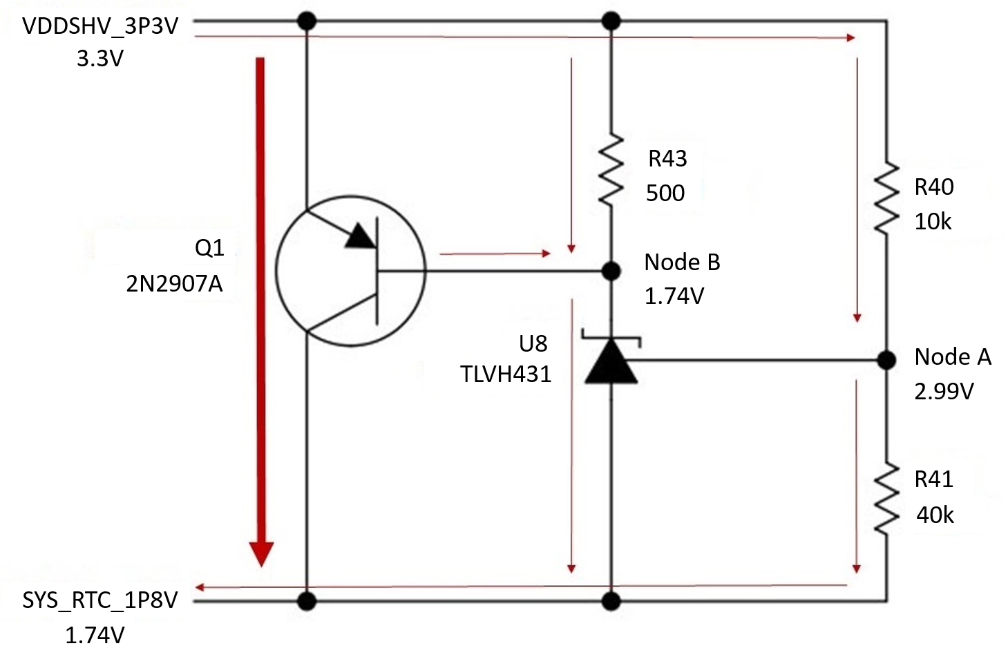
Now, let’s understand the behavior of clamping circuit when the voltage difference between its two power rails is greater than 1.55V. Let’s assume VDDSHV_3P3V is at 3.3V and SYS_RTC_1P8V is at 1.74V as shown in Figure 4 (Fixing the voltage will help us understand the circuit better). Hence, the voltage difference between the two power rails becomes 1.56V (3.3V – 1.74V = 1.56V).
When SYS_RTC_1P8V is at 1.74V, the voltage at node A will be 2.99V (i.e., 2.99V-1.74V = 1.25V with respect to SYS_RTC_1P8V rail). As a result, U8 (TLVH431) turns ON and sinks current from node B. This will lower the voltage at node B to 1.74V and the voltage difference between the base and emitter of Q1 will exceed 0.4V. Hence, Q1 will turn ON and current begins to flow from VDDSHV_3P3V rail to SYS_RTC_1P8V rail. This will increase the voltage of SYS_RTC_1P8V rail to 1.75V. The voltage at node A with respect to ground will now become 1.24V (2.99V – 1.75V = 1.24V) and U8 will turn OFF. So, Q1 will turn OFF and current flow from VDDSHV_3P3V to SYS_RTC_1P8V will cease.
This cycle continues until one or both of the voltage rails drop down to 0V at the end of the power down sequence. Now, this is an idealized analysis so in the real operation there will be some overshoot and undershoot but based on the voltage ripple should be less than ±5%.
Phase 3 – End of AM335x power down sequence (Clamping circuit back to standby):
The clamping circuit will operate in this phase when the AM335x is almost at the end of its power down sequence and after SYS_RTC_1P8V drops down to 0V while VDDSHV_3P3V is still at 1.55V as shown in Figure 5.
When SYS_RTC_1P8V is at 0V, the voltage at node A will be 1.24V. As a result, U8 (TLVH431) turns OFF and will not sink current from node B. This will lower the voltage at node B and the voltage difference between the base and emitter of Q1 will be less than 0.4V. Hence, Q1 will turn OFF. This is similar to Phase 1 where both U8 and Q1 are off.
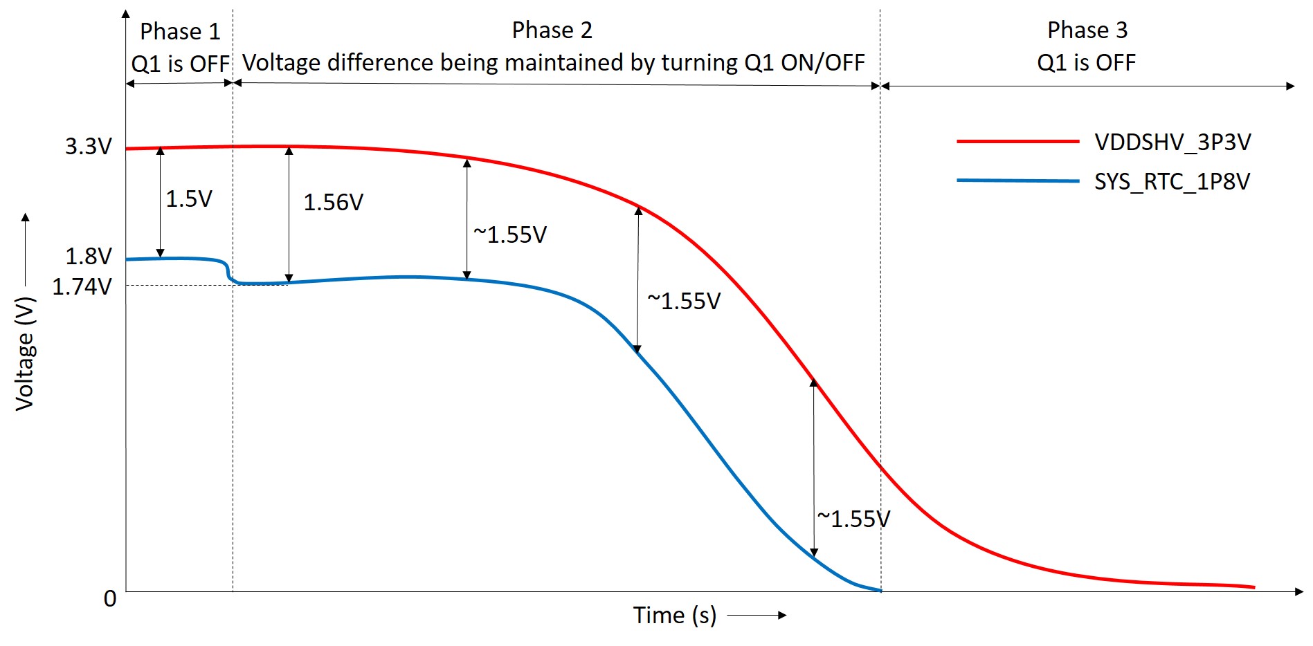
The operation of clamping circuit and its three phases can be better understood with the help of a voltage vs time graph as shown in Figure 6.
Phase 1: The clamping circuit will be in standby and Q1 is OFF.
Phase 2: Initially, the clamping circuit will turn ON when the voltage difference between the given two power rails increases to 1.56V (shown at the beginning of Phase 2 in Figure 6). After this, the clamping circuit will actively maintain the voltage difference between VDDSHV_3P3V and SYS_RTC_1P8V at approximately 1.55V.
Phase 3: The clamping circuit will go back to standby mode since SYS_RTC_1P8V will drop down to 0V while VDDSHV_3P3V is at 1.55V and the difference between the two voltage rails is 1.55V.
Let’s build the schematic of the clamping circuit as shown in Figure 7.
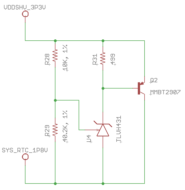
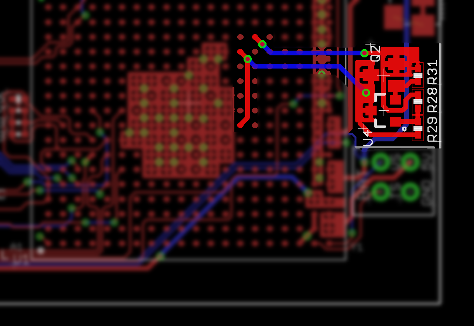
For this design, we used copper pours as well as 15 mil traces so that there is good electrical as well as thermal connections.
Since we only wanted to put components on a single side of the board for this design, the power outputs were routed to the clamping circuit as shown in Figure 8. However, if placing components on the back side of the board, clamping circuit can go directly under the power connections.
| << Return to “OSD335x Power Management” | Continue to “OSD335x ESD Protection” >> |
