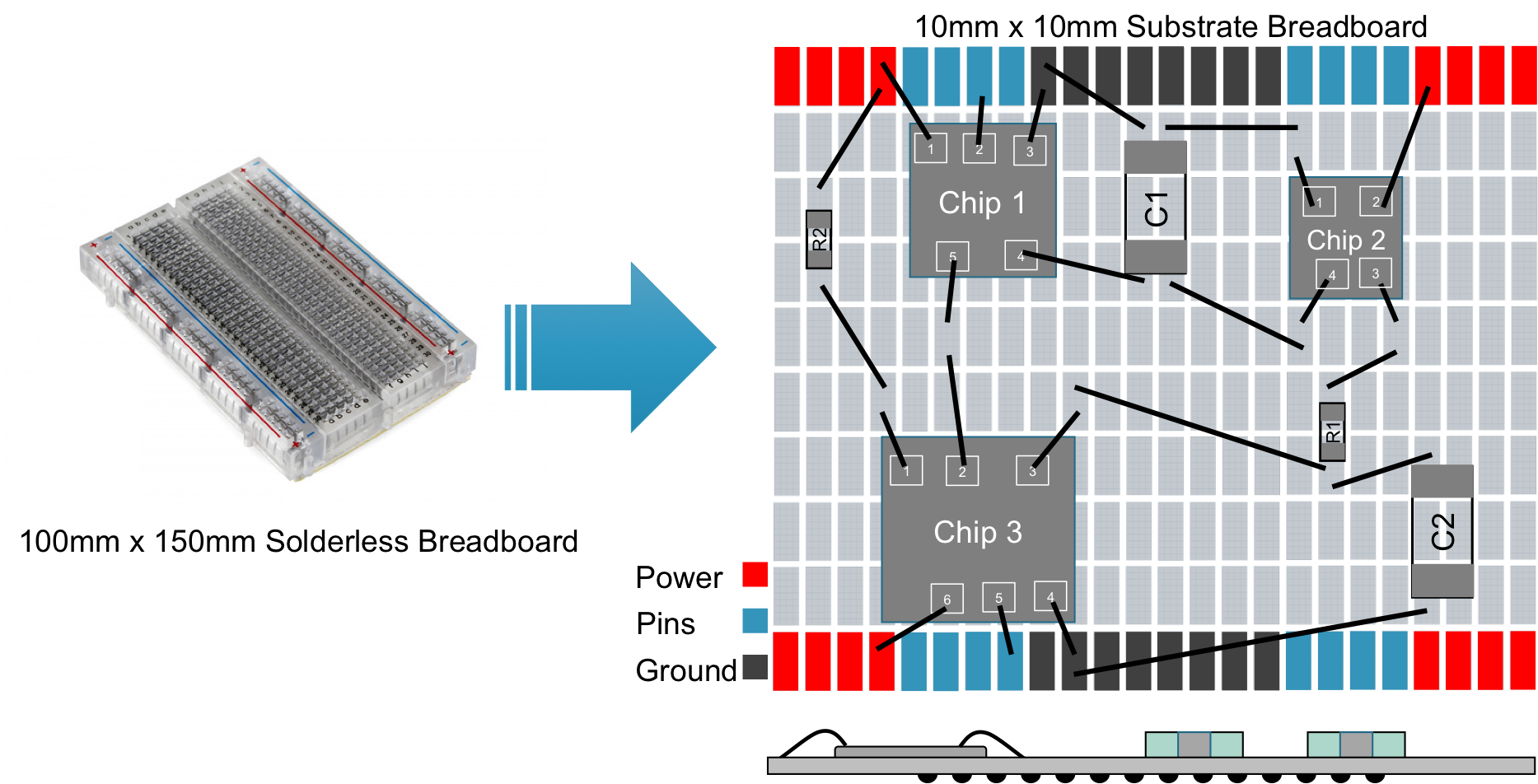
As Moore’s Law approaches retirement age[1][2], the technological advances wrought through the improvements in silicon process technology are staggering. The ability to tailor a process for high power, high voltage power electronics vs low power, low voltage, extremely dense microprocessor and memories enables the proliferation of technology in the age of the Internet of Things (IoT). However, for all the advancements, each silicon component can only have one process; a compromise necessary for each circuit that needs to be optimally built. Where Moore’s Law left off from the perspective of the individual component, packaging technology has taken up the reigns. Packaging technologies are able push the boundaries of form, fit, and function beyond that which is possible with System on a Chip (SoC) technology. Systems in a Package (“SiP”s) can enable new levels of integration and size reduction for embedded systems[3][4]. However, like the technologies that have come before it, SiPs require enormous investments of design time and effort. In this paper, we introduce the future of SiP: the Universal Connection Matrix (UCM) . This allows for faster design and prototyping with SiP devices. Instead of large, monolithic designs, the UCM provides a breadboard in a package.
It is always worth our while to review the state of the art of integrated circuit technology. As one who has been in the middle of it for over 40 years, it is interesting to see how we have advanced the technology by driving the learning curve, exploiting the physics of silicon and creating new ways to design billions of transistors into functioning, reliable, affordable products. The products that have revolutionized the world we live in.
I believe we are only at the beginning of a transition from integration at the component level to integration at the system level. The new heterogeneous integration method known at System-in-Package (SiP) will be the technology of choice.
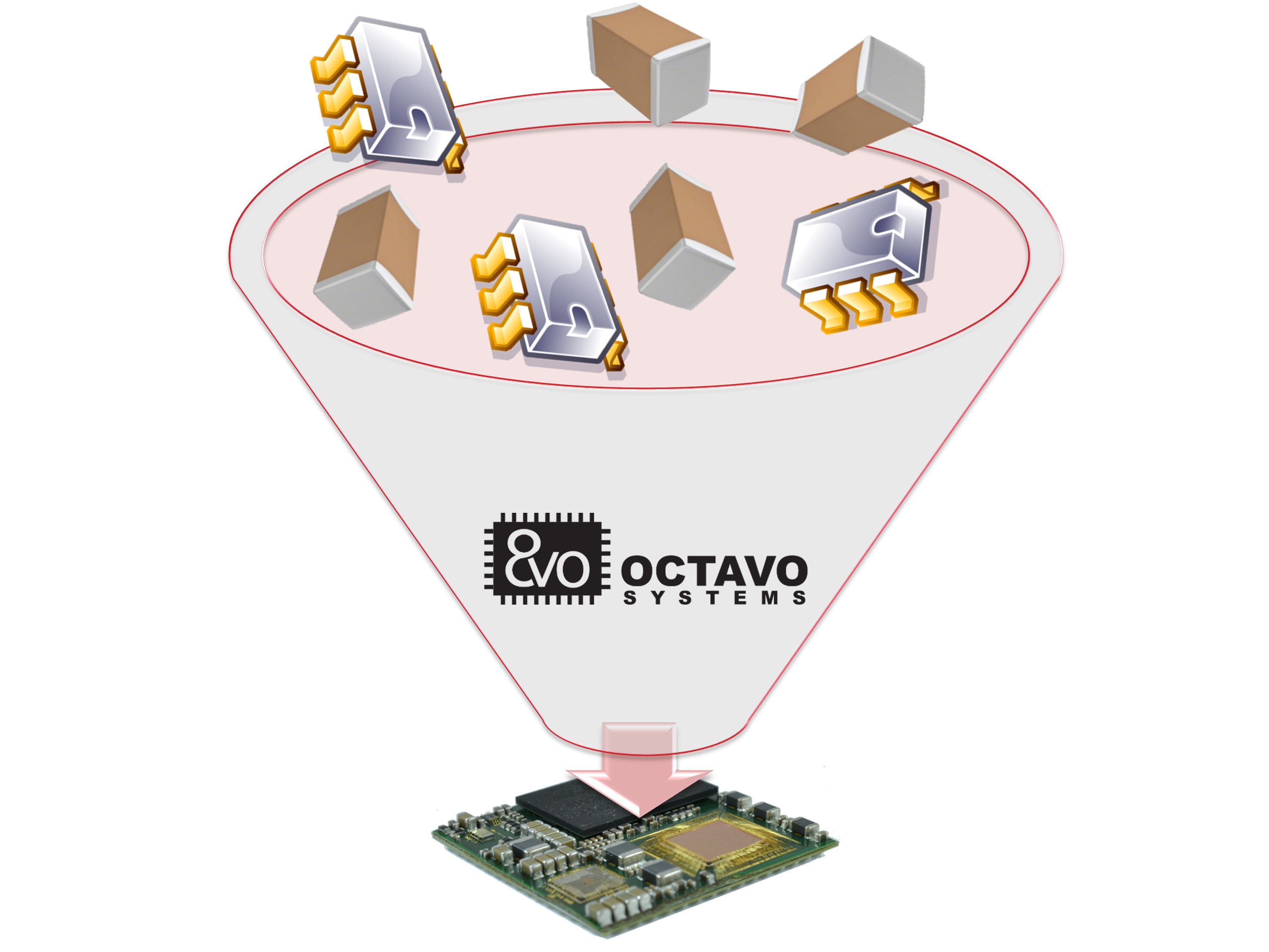
That is why Octavo’s products and strategy are based on this proven technology platform known as SiP. Although the technologies associated with SiP integration have been around for over a decade and are well established in the semiconductor industry, they have not been exploited for system integration. Our goal is to develop these existing technologies, along with new concepts, to deliver to you unprecedented integration and design flexibility.
SiP technology will help increase the performance of products while increasing their reliability.
One of the key benefits delivered by System-In-Package (SiP) technology is the savings realized in the Printed Circuit Board (PCB) Assembly process. This is a benefit that is commonly overlooked by designers on the front end. Typically, they only look at the cost of the individual components on the Bill of Material (BOM) and don’t consider the cost of assembly. With System-In-Package technology, the number of components that need be placed during the assembly process can be significantly reduced. This reduction decreases the component set up time and actual time spent on the Pick and Place machine. Simultaneously driving down the assembly cost and the total cost of the finished product. (Read More…)