OSD335x Schematic Checklist – AM335x System in Package
Published On: May, 30, 2019 By: Eshtaartha Basu

This document provides a generic OSD335x schematic checklist to help users review designs built around the OSD335x, the AM335x System in Package, Family of Devices. Going through this checklist before or during the schematic design phase will help avoid some common pitfalls. This OSD335x schematic checklist targets a generic embedded system and is not exhaustive. Each design is unique and your custom design may require additional in-depth verification to validate its overall functionality.
The first section of the OSD335x schematic checklist document consists of various sub system checklists to help you validate your design. The second section (i.e., Appendix) consists of supplemental information which will be referenced from the first section to further aid your design validation.
Get updates to this application note and all of our documentation
"*" indicates required fields
| ITEM | SECTION | SCHEMATIC CHECKLIST TOPIC | |
|---|---|---|---|
| 1 | 2.1 | Prepared to Check your Power Design? | |
| 2 | 2.2 | Adding an Oscillator? | |
| 3 | 2.2 | Ready to Reset? | |
| 4 | 2.3 | Best Boot Configuration Settings? Make sure your design can boot properly. | |
| 5 | 2.4 & 2.6 | Planning for Peripheral Success? Check your USB, I2C, UART, SPI and more in this section. | |
| 6 | 2.6 | Prepping for Peripheral Success? Leaving off some peripherals? Let's check your IO in this section. | |
| 7 | 2.5 | Enabling eMMC? Need non-volatile storage? Are meeting the requirements? | |
| 8 | 2.6 | Ready to Juggle JTAG? Check for a properly connected JTAG to be a great debug resource. | |
| 9 | 2.6 | Excited about EEPROM? Let's check your EEPROM WP pin. | |
| 10 | 3.5 | Have you used your good-luck charm? (Having ten things on a list made marketing happy.) |
Table of Contents
1.Introduction
2.OSD335x Schematic Checklists
2.1Essential Connections and Power Design
2.2Reset and Clock
2.3Boot Configuration
2.4USB
2.5eMMC
2.6Other Interfaces
3.Appendix
3.1Use Cases
3.1.1Power Input
3.1.2Reset Circuit
3.2Reference Figures
3.2.1Minimal Connections
3.2.2Crystal Circuit Example
3.2.3Boot Configuration Example
3.2.4eMMC Pinout
3.3Useful App Notes and Links
3.3.1Power Design
3.3.2Reset and Clock
3.3.3Boot Configuration
3.3.4USB
3.3.5eMMC
3.3.6GPIO and Other Interfaces
3.4References
4.Revision History of this Document
![]()
![]() A PDF version of this App Note can be found here.
A PDF version of this App Note can be found here.

2. OSD335x Schematic Checklists
2.1 Essential Connections and Power Design
Table 1 Essential Connections and Power Design Checklist - Mandatory
| Topic No. | OSD335x | OSD335x-SM | OSD335x C-SiP | SCHEMATIC CHECKLIST TOPIC - Mandatory |
|---|---|---|---|---|
| PD1 | ?? | ?? | ?? | Input Power Connections: Choose a power input use case from Table 13 based on design requirements and implement mandatory connections |
| PD2 | ?? | ?? | ?? | In-Rush Current: The power source connected to a power input must be able to supply the necessary in-rush current: VIN_AC - ~1.2A; VIN_USB - ~0.5A; VIN_BAT - ~0.35A |
| PD4 | ?? | ?? | ?? | External Capacitance: ~50uF of external capacitance required on SYS_VOUT |
| PD5 | ? | ?? | ?? | IO Voltage: Connect each of the six VDDSHVx pins to either SYS_VDD3_3P3V (for 3.3V I/O) or SYS_VDD_1P8V (for 1.8V I/O)(1) (See Pin Attributes section of AM335x datasheet to find the VDDSHVx domain of a pin) |
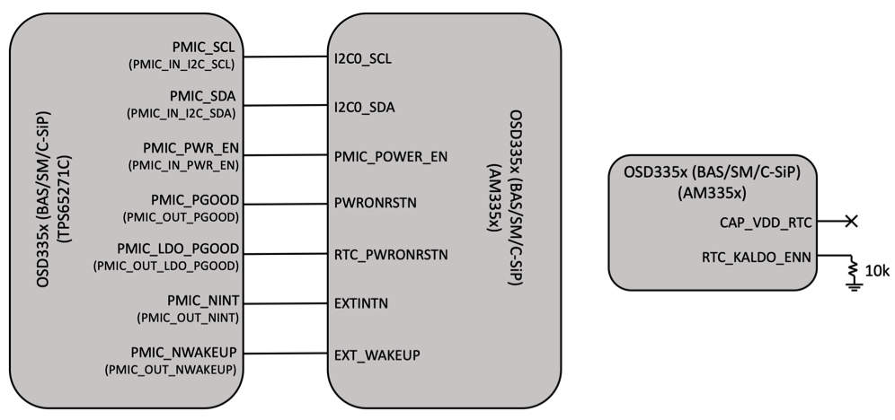
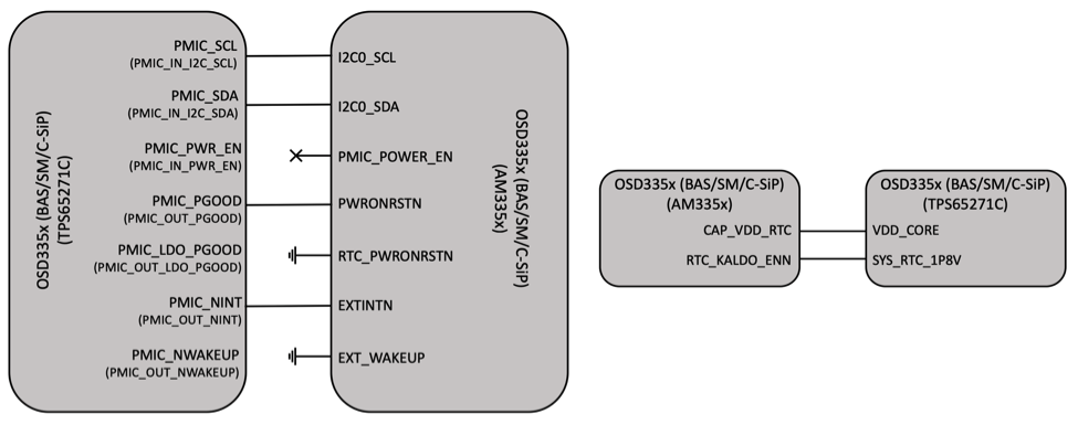
| PD6 | ?? | ?? | ?? | Processor – PMIC Connections: See Figure 5 and Figure 6 for mandatory connections between TPS65217C (PMIC) and AM335x processor based on required RTC mode |
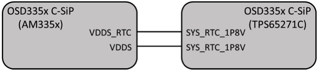
| PD7 | ? | ? | ?? | RTC Power Connections: See Figure 7 for VDDS and VDDS_RTC power connections |
| PD8 | ? | ? | ?? | eMMC Power Connections: Connect EMMC_VCC and EMMC_VCCQ (2) to SYS_VDD1_3P3V |
(1) In OSD335x-BAS, all VDDSHVx signals are internally connected to SYS_VDD3_3P3V. Therefore, level shifters are required for any I/O voltage other than 3.3V.
(2) If necessary, can power eMMC using external 3.3V supply instead of SYS_VDD1_3P3V.
Table 2 Essential Connections and Power Design Checklist - Recommended
| Topic No. | OSD335x | OSD335x-SM | OSD335x C-SiP | SCHEMATIC CHECKLIST TOPIC - Recommended |
|---|---|---|---|---|
| PD9 | ?? | ?? | ?? | Power Budget: Power Budget: Create a Power Budget for your design using the power app notes: Power Application Note for OSD335x-BAS/IND Power Application Note for OSD335x-BSM/ISM |
| PD10 | ?? | ?? | ?? | Clamping Circuit: Review OSD335x Clamping Circuit app note to determine if your application needs the clamping circuit |
| PD11 | ?? | ?? | ?? | Test Points: Add a test point on each signal if possible: Boot Signals: PMIC_POWER_EN, RTC_PWRONRSTN, EXT_WAKEUP, EXTINTN Reset/Control Signals: PWRONRSTN, WARMRSTN, PMIC_NRESET (1), SYS_VDD1_CTL (2) Output Power Rails: SYS_VOUT, SYS_VDD1_3P3V, SYS_VDD2_3P3V, SYS_VDD3_3P3V (1), SYS_RTC_1P8V, SYS_VDD_1P8V |
| PD12 | ?? | ?? | ?? | App Notes: Understand if any app notes listed under section 3.3.1 applies to your design |
(1) Not available on OSD335x-BAS.
(2) Only available on OSD335x C-SiP.
2.2 Reset and Clock
Table 3 Reset and Clock Checklist - Mandatory
| Topic No. | OSD335x | OSD335x-SM | OSD335x C-SiP | SCHEMATIC CHECKLIST TOPIC - Mandatory |
|---|---|---|---|---|
| RC1 | ?? | ?? | ?? | Reset Connections: Choose a reset circuit use case from section 3.1.2 based on design requirements and implement mandatory connections |
| RC2 | ?? | ?? | ?? | OSC1 Unconnected: If the AM335x Real-Time Clock (RTC) is not used, leave pins OSC1_IN, OSC1_OUT, and OSC1_GND floating |
Table 4 Reset and Clock Checklist - Recommended
| Topic No. | OSD335x | OSD335x-SM | OSD335x C-SiP | SCHEMATIC CHECKLIST TOPIC - Recommended |
|---|---|---|---|---|
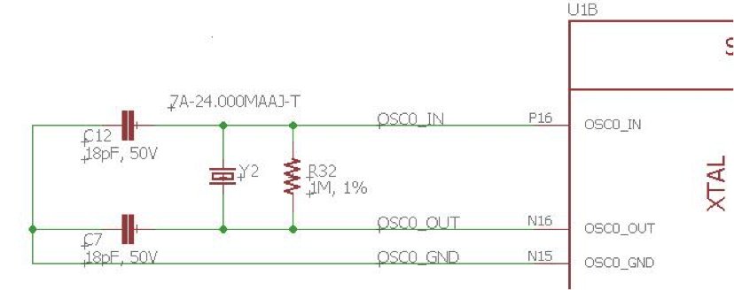
| RC3 | ?? | ?? | ?? | Oscillator Connections: Use the oscillator circuit shown in Figure 8 for OSC0 and OSC1 clock design (1). This will allow tuning of the crystal oscillator if needed |
| RC4 | ?? | ?? | ?? | App Notes: Understand if any app notes listed under section 3.3.2 applies to your design |
(1) In OSD335x C-SiP, 24MHz MEMS Oscillator is internally connected to OSC0 of AM335x. The MEMS Oscillator is enabled by an internal pull-up. Hence, add a test point to OSC0_CTL to have the flexibility of external control.
2.3 Boot Configuration
Table 5 Boot Configuration Checklist - Mandatory
| Topic No. | OSD335x | OSD335x-SM | OSD335x C-SiP | SCHEMATIC CHECKLIST TOPIC - Mandatory |
|---|---|---|---|---|
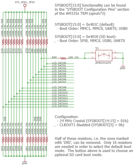
| BC1 | ?? | ?? | ? | Oscillator Frequency: Set SYSBOOT [15:14] to OSC0 crystal / oscillator frequency (1) 0b00 19.2 MHz 0b01 24 MHz 0b10 25 MHz 0b11 26 MHz |
| BC2 | ?? | ?? | ?? | CLKOUT1 Default Setting: Set SYSBOOT [5] high only if CLKOUT1 (pin XDMA_EVENT_INTR0) is used during boot for OSC0 frequency output |
| BC3 | ?? | ?? | ?? | Boot Mode:Set SYSBOOT [4:0] to the appropriate value from Table 26-7 of the AM335x TRM to support the required boot peripherals for the design. For example, some common boot modes include: Value Peripheral Boot Sequence 0b11000 SPI0 ? MMC0 ? USB0 ? UART0 0b11100 MMC1 ? MMC0 ? UART0 ? USB0 |
| BC4 | ?? | ?? | ?? | Other Pins:Pull other SYSBOOT pins low unless they are needed for the Boot Mode |
| BC5 | ?? | ?? | ?? | SYSBOOT Conflicts: Check that there are no pull ups, pull downs or drivers on the SYSBOOT pins that could incorrectly modify the value of SYSBOOT before the SYSBOOT pins are sampled (i.e. reset is de-asserted) |
(1) In OSD335x C-SiP, SYSBOOT [15:14] = 0b01 to match the 24 MHz MEMS oscillator frequency within the device.
Table 6 Boot Configuration Checklist - Recommended
| Topic No. | OSD335x | OSD335x-SM | OSD335x C-SiP | SCHEMATIC CHECKLIST TOPIC - Recommended |
|---|---|---|---|---|
| BC6 | ?? | ?? | ?? | Resistors: Use ~100K resistors to set SYSTBOOT pins high/low to reduce static power dissipation. Use stronger resistors only if needed. Boot configuration example shown in Figure 9 |
| BC7 | ?? | ?? | ?? | App Notes:Understand if any app notes listed under section 3.3.3 applies to your design |
2.4 USB
Table 7 USB Checklist - Mandatory
| Topic No. | OSD335x | OSD335x-SM | OSD335x C-SiP | SCHEMATIC CHECKLIST TOPIC - Mandatory |
|---|---|---|---|---|
| UB1 | ?? | ?? | ?? | USB VBUS Sense Input: USBx_VBUS is a voltage sense input and NOT a power output pin. Check that a valid voltage (>=4.4V) is present on the pin to enable the USBx peripheral. |
| UB2 | ?? | ?? | ?? | USB Termination Resistors: There should be no series resistors on USBx_DP and USBx_DM lines. Additionally, do not add any external capacitors to the USB lines |
| UB3 | ?? | ?? | ?? | USB Routing:USBx_DP and USBx_DM traces must be length matched between the OSD335x and the USB endpoint or connector with minimal stubs |
| UB4 | ?? | ?? | ?? | USB Host Mode Power:Connect USBx_DRVVBUS to enable pin of external power switch/regulator to external USB devices when port in Host mode |
| UB5 | ?? | ?? | ?? | USB ID Connection: USBx_ID pin values: Host Mode Pulled to Ground Client Mode Floating OTG Mode Connected to USB client connector |
Table 8 USB Checklist - Recommended
| Topic No. | OSD335x | OSD335x-SM | OSD335x C-SiP | SCHEMATIC CHECKLIST TOPIC - Recommended |
|---|---|---|---|---|
| UB6 | ?? | ?? | ?? | App Notes: Understand if any app notes listed under section 3.3.4 applies to your design |
2.5 eMMC
Table 9 eMMC Checklist - Mandatory
| Topic No. | OSD335x | OSD335x-SM | OSD335x C-SiP | SCHEMATIC CHECKLIST TOPIC - Mandatory |
|---|---|---|---|---|
| MC1 | ?? | ?? | ? | eMMC Pull-up Resistors: Use 10K pull-up resistors on RST#, CMD, and all DAT signals |
Table 10 eMMC Checklist - Recommended
| Topic No. | OSD335x | OSD335x-SM | OSD335x C-SiP | SCHEMATIC CHECKLIST TOPIC - Recommended |
|---|---|---|---|---|
| MC2 | ?? | ?? | ? | eMMC Termination Resistors: Include a 22ohm series resistor on MMCx_CLK signals close to the processor to eliminate possible reflections and false clock transitions |
| MC3 | ?? | ?? | ? | eMMC Connections:The AM335x supports the MMC v4.3 interface so only those signals must be connected. Any MMC v5.x signals do not need to be connected (1) |
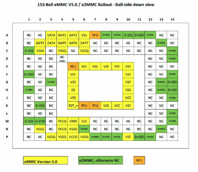
| MC4 | ?? | ?? | ? | eMMC Routing:In Figure 10, the “No Connect” (NC) pins can be routed through but “Reserved for Future Use” (RFU) pins should not be routed through to allow larger trace widths when routing the eMMC |
| MC5 | ?? | ?? | ? | App Notes:Understand if any app notes listed under section 3.3.5 applies to your design |
(1) OSD335x C-SiP comes with an integrated eMMC. Adding an external eMMC is not necessary.
2.6 Other Interfaces
Table 11 Other Interfaces Checklist - Mandatory
| Topic No. | OSD335x | OSD335x-SM | OSD335x C-SiP | SCHEMATIC CHECKLIST TOPIC - Mandatory |
|---|---|---|---|---|
| IO1 | ?? | ?? | ?? | Pin Mapping: If porting from legacy AM335x design, verify the pin mapping between AM335x and OSD335x using OSD335x Family Pin Assignments app note |
| IO2 | ?? | ?? | ?? | Pin Muxing:Verify pin mux settings using TI Pin Mux Tool. All chosen pins of a peripheral must belong to the same IO set |
| IO3 | ?? | ?? | ?? | UART RequirementsImplement Null Modem for all UART devices (i.e. TX -> RX; RX -> TX; CTS -> RTS; RTS -> CTS; DTR -> DSR; DSR -> DTR) |
| IO4 | ?? | ?? | ?? | SPI Requirements:Each SPI device should have its own Chip Select (CS) |
| IO5 | ?? | ?? | ?? | I2C requirements:All I2C busses must be pulled up(1) |
| IO6 | ?? | ?? | ?? | JTAG Requirements:EMU0 and EMU1 pins must be connected to the JTAG debugger. Add 4.75K pullup resistors on both pins (2) |
| IO7 | ?? | ?? | ?? | EEPROM Write Protect:Connect EEPROM_WP pin to either an external test point or ground jumper or external control logic. EEPROM_WP needs to pulled low in order to write to the EEPROM |
(1) I2C0 pins have internal 4.7K pull up resistors. However, we recommend adding external pull up resistor footprints for I2C0 if more than two (2) external devices use I2C0 to allow for stronger pull ups.
(2) The internal pull-ups on EMU0 and EMU1 are typically weak and therefore external pullup resistors (~4.75K) are recommended. See EMU Considerations section of XDS Target Connection Guide.
Table 12 Other Interfaces Checklist - Recommended
| Topic No. | OSD335x | OSD335x-SM | OSD335x C-SiP | SCHEMATIC CHECKLIST TOPIC - Recommended |
|---|---|---|---|---|
| IO8 | ?? | ?? | ?? | Unused IO: Leave unused IO peripheral pins floating (2) |
| IO9 | ?? | ?? | ?? | Advanced JTAG:Connect EMU2, EMU3 and EMU4 to JTAG debug header if advanced JTAG features (HS-RTDX, Core Trace, System Trace, etc.) of high-end debuggers are required |
| IO10 | ?? | ?? | ?? | MII Termination Resistors: Add termination resistor footprints for TX and RX lines of MII/RMII/RGMII interfaces. |
| IO11 | ?? | ?? | ?? | Cape Header Compatibility:If BeagleBone® Cape Header compatibility is not required, remove the resistor MUXes between pins GPMC_A0 and GPMC_CSN3; and ECAP0_IN_PWM0_OUT and MCASP0_ACLKR (Seen in OSD335x Reference Designs) |
| IO12 | ?? | ?? | ?? | Static Signals with ADC:If ADC is used to monitor static voltages (e.g., 3.3V rail), then you do not need any external filter capacitors / resistors between SYS_ADC_1P8V, VSSA_ADC, VREFN and VREFP |
| IO13 | ?? | ?? | ?? | Unused ADC:If the ADC module is not used, connect VREFP, VREFN(1), AIN [7:0] and VSSA_ADC terminals to system ground |
| IO14 | ?? | ?? | ?? | App Notes:Understand if any app notes listed under section 3.3.6 applies to your design |
(1) VREFN is not externally accessible on OSD335x-BAS.
(2) Exceptions: Topic IO13.
3. OSD335x Schematic Checklist Appendix
3.1 Use Cases
3.1.1 Power Input
Table 13 Power Input Use Cases
| Use Case | Power Input: VIN_AC | Power Input: VIN_USB | Power Input: VIN_BAT | Source Connection | Sink Connection |
|---|---|---|---|---|---|
| 1 | ? | ? | ?? | Connect VIN_AC Connect VIN_USB Connect VIN_BAT Connect PMIC_TS | to Ground (1) to Ground (1) to PMIC_BAT_SENSE and battery (4) to NTC thermistor of battery pack (5) |
| 2 | ? | ?? | ? | Connect VIN_AC Connect VIN_USB Connect VIN_BAT Connect PMIC_TS | to Ground to VBUS of USB client connector (2) to PMIC_BAT_SENSE to nothing (i.e. leave floating) |
| 3 | ? | ?? | ?? | Connect VIN_AC Connect VIN_USB Connect VIN_BAT Connect PMIC_TS | to Ground to VBUS of USB client connector (2)< to PMIC_BAT_SENSE and battery (4) to NTC thermistor of battery pack (5) |
| 4 | ?? | ? | ? | Connect VIN_AC Connect VIN_USB Connect VIN_BAT Connect PMIC_TS | to 5V DC Power Supply (3) to Ground to PMIC_BAT_SENSE to nothing (i.e. leave floating) |
| 5 | ?? | ? | ?? | Connect VIN_AC Connect VIN_USB Connect VIN_BAT Connect PMIC_TS | to 5V DC Power Supply to Ground to PMIC_BAT_SENSE and battery (4) to NTC thermistor of battery pack (5) |
| 6 | ?? | ?? | ? | Connect VIN_AC Connect VIN_USB Connect VIN_BAT Connect PMIC_TS | to 5V DC Power Supply to VBUS of USB client connector (2) to PMIC_BAT_SENSE to nothing (i.e. leave floating) |
| 7 | ?? | ?? | ?? | Connect VIN_AC Connect VIN_USB Connect VIN_BAT Connect PMIC_TS | to 5V DC Power Supply to VBUS of USB client connector (2) to PMIC_BAT_SENSE and battery (4) to NTC thermistor of battery pack (5) |
(1) See Figure 62 of TPS65217C datasheet.
(2) Increasing USB input-current limit may be necessary. See section 8.6.3 of TPS65217C datasheet.
(3) See Figure 61 of TPS65217C datasheet.
(4) DC Power supply can be used in lieu of a battery if no OVP is required
(5) 10K resistor to ground may be substituted if battery pack has no NTC thermistor (i.e. temperature monitoring)
3.1.2 Reset Circuit
The different Reset Configurations supported by the OSD335x Family of Devices are described below. Use the Reset Circuit Selection Guide (Figure 1) to choose a Reset Circuit Use-Case that best suits your design requirement. (Please note that in the AM335x Technical Reference Manual, Section 8.1.7, the WARMRSTN signal may also be called nRESETIN_OUT):
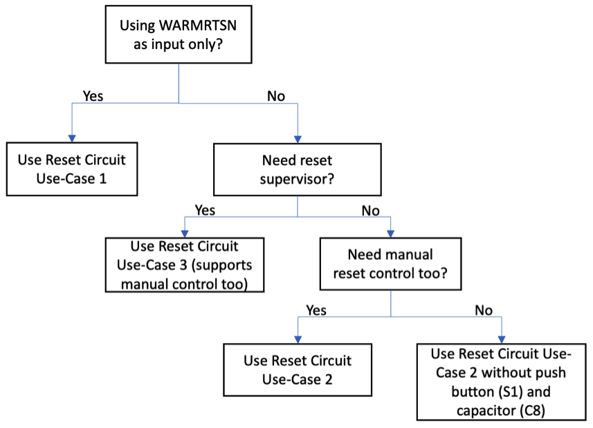
- Use-Case 1: In this Use-Case:
- WARMRSTN is used as input.
- WARMRSTN is controlled by PWRONRSTN.
- No external components are controlled by WARMRSTN
- No manual control of WARMRSTN is available.
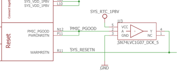
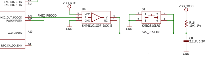
- Use-Case 2: In this Use-Case:
- WARMRSTN is used as both input and output.
- WARMRSTN is controlled by PWRONRSTN.
- The reset lines of external components are tied to WARMRSTN.
- Manual control of WARMRSTN is made available.
(NOTE: OSD335x C-SiP integrates an open drain buffer internally connected to PWRONRSTN. See OSD335x C-SiP Reset Circuitry section of OSD335x C-SiP Design Tutorial).
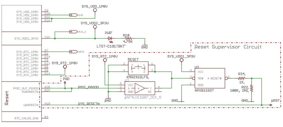
- Use-Case 3: In this Use-Case:
- A dedicated Reset Supervisor circuit is used to manage reset circuitry.
- WARMRSTN is used as both input and output.
- WARMRSTN is controlled by PWRONRSTN.
- The reset lines of external components are tied to WARMRSTN.
- Manual control of WARMRSTN (and debouncing of push button) is made available through reset supervisor.
(NOTE: OSD335x C-SiP integrates an open drain buffer internally connected to PWRONRSTN. See OSD335x C-SiP Reset Circuitry section of OSD335x C-SiP Design Tutorial).

3.2 Reference Figures
3.2.1 Minimal Connections
3.2.2 Crystal Circuit Example
3.2.3 Boot Configuration Example
3.2.4 eMMC Pinout
3.3 OSD335x Schematic Checklist Useful App Notes and Links
3.3.1 Power Design
- OSD335x-BAS/IND Power Application Note: https://octavosystems.com/app_notes/osd335x-power-application-note/
- OSD335x Power Inputs and Outputs: https://octavosystems.com/app_notes/osd335x-design-tutorial/bare-minimum-boot/power-input-ouput/
- OSD335x Power Management: https://octavosystems.com/app_notes/osd335x-design-tutorial/bare-minimum-boot/power-management/
- OSD335x-SM Power Application Note: https://octavosystems.com/app_notes/osd335x-sm-power-application-note/
- OSD335x C-SiP Power Application Note: https://octavosystems.com/app_notes/osd335x-c-sip-power-application-note/
3.3.2 Reset and Clock
- OSD335x Reset Circuitry: https://octavosystems.com/app_notes/osd335x-design-tutorial/bare-minimum-boot/reset-circuitry/
- OSD335x Clock Circuitry: https://octavosystems.com/app_notes/osd335x-design-tutorial/bare-minimum-boot/clock-circuitry/
- “Clock Specifications” in AM335x Datasheet: http://www.ti.com/lit/ds/symlink/am3358.pdf
3.3.3 Boot Configuration
- AM335x TRM “SYSBOOT Configuration Pins”: https://www.ti.com/lit/ug/spruh73p/spruh73p.pdf
- OSD335x Peripheral Circuitry tutorial: https://octavosystems.com/app_notes/osd335x-design-tutorial/bare-minimum-boot/power-management/
3.3.4 USB
- OSD335x Lesson 2: USB Circuitry: https://octavosystems.com/app_notes/osd335x-design-tutorial/osd335x-lesson-2-minimal-linux-boot/osd335x-lesson-2-usb-circuitry/
3.3.5 eMMC
- OSD335x eMMC Application Note: https://octavosystems.com/app_notes/designing-for-flexibility-around-emmc/
- OSD335x Design Tutorial Lesson 2: Adding Non-Volatile Storage https://octavosystems.com/app_notes/osd335x-lesson-2-adding-non-volatile-storage/
3.3.6 GPIO and Other Interfaces
- OSD335x Peripheral Circuitry tutorial: https://octavosystems.com/app_notes/osd335x-design-tutorial/bare-minimum-boot/peripheral-circuitry/
- Texas Instruments JTAG resource: http://dev.ti.com/tirex/#/?link=Development%20Tools%2FDebug%20Probes%2FXDS%2FDocuments%2FJTAG%20Connectors
- OSD3358-SM-RED Schematics – PDF: https://octavosystems.com/docs/osd3358-sm-red-schematics-pdf/
3.4 OSD335x Schematic Checklist References
- OSD335x-BAS/IND Datasheet: https://octavosystems.com/docs/osd335x-datasheet/
- OSD335x-BSM/ISM Datasheet: https://octavosystems.com/docs/osd335x-sm-datasheet/
- OSD335x-BCB/ICB Datasheet: https://octavosystems.com/docs/osd335x-c-sip-datasheet/
- AM335x Schematic Checklist: http://processors.wiki.ti.com/index.php/AM335x_Schematic_Checklist
- OSD335x Power Application Note: https://octavosystems.com/app_notes/osd335x-sm-power-application-note/
- OSD335x Design Tutorial Series: https://octavosystems.com/app_notes/osd335x-design-tutorial/
- AM335x Datasheet: http://www.ti.com/lit/ds/symlink/am3358.pdf
- TPS65217C PMIC Datasheet: http://www.ti.com/lit/ds/symlink/tps65217.pdf
- Powering AM335x with TPS65217x: http://www.ti.com/lit/ug/slvu551i/slvu551i.pdf
- Designing for Flexibility around eMMC: https://octavosystems.com/app_notes/designing-for-flexibility-around-emmc/
- org® PocketBeagle® https://www.beagleboard.org/pocket
3.5 Contact Us
Please contact us on the forums for assistance with any checklist items or to tell us more things you’d like to see on this list. Our team is ready with more than a good-luck charm to help you with your designs. https://octavosystems.com/forums/
4. Revision History
| Revision Number | Revision Date | Changes | Author |
|---|---|---|---|
| 3 | 5/30/2019 | Restructured document for readability with charts, added C-SiP info and USBx-VBUS | E. Basu |
