
SiP Technology: A solution to a passive problem
It is always interesting when a new integration concept like System in Package (SiP) technology gives opportunity to innovate beyond the obvious. One of those opportunities which has no effect on system designers or component designers but is unique to a SiP designer is the handling of the bulk and bypass capacitors.
But before we get to the topic of capacitor reduction, let me take a moment to remind all of us of some of those new integration concepts:
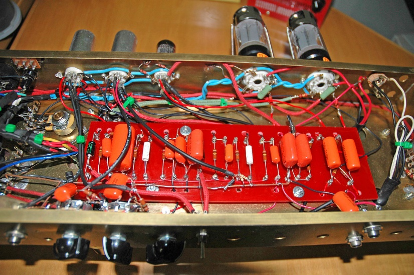
- Point to Point wiring (PtP): this concept is still being used in guitar amplifiers. Figure 1 will remind you of the concept.
- Printed Circuit boards (PCB). Once components could be attached to a PCB, PtP began to take a back seat. Note Figure 1 also has a PCB included.
- Integrated circuits with the ultimate being a System on Chip (SoC)
- System in Package (SiP)
OK, with that behind us, let’s return to the SiP technology opportunity for innovation.
Component vendors (e.g., microprocessor and memory suppliers) are careful to specify how many and what kind of bulk and bypass capacitors are needed for proper operation of their component. These specifications are generally determined to allow for correct operation over the full range of the power rails, over the temperature range, and the worst case distance between the power source and their component.
As a quick background, the bulk capacitors are designed to prevent voltage sag on the rails due to current variations. Bypass capacitors are designed to reduce the noise on the voltage rails which effect signal integrity.
That is where the uniqueness of a SiP device changes the requirements. When the voltage source is made part of the SiP design using a Power Management Integrated Circuit (PMIC), the various rails can be managed to minimize the effect of voltage sag on the components in the SiP and, because the trace distances between components is reduced from centimeters to millimeters, the amount of noise on the various rails is minimized. Both of these effects give opportunity impact the bulk capacitor and the bypass capacitor requirements.
Although this opportunity has little or no effect on the resulting system or component designs, it is an interesting concept for all of us to appreciate. So with this as an introduction, let me tell a quick story of the “aha” moment we had at Octavo Systems with our OSD3358 family of devices.
The Aha moment
One of our engineers asked a crazy question: “Would it be possible to reduce the number of capacitors in our OSD3358?” The reason for the reduction was obviously to reduce cost and size of the SiP. (Note, reducing size could be replaced by the idea of adding components to the SiP.)
Once our design team concluded that it might be, an experiment was designed to test the hypothesis. The experiment had three versions of the same SiP product, the OSD3358-BAS. Figure 2 shows the makeup of the three versions. The first group (CNTL) had the number of capacitors listed in the first column, which included a full complement of recommended capacitors from the data sheets for the components used in the design. The second group (SWRa) had the number of capacitors listed in the second column, reducing the number of capacitors from 123 to 75. Even with the reduced numbers of capacitors, we still expected it to be a viable operating solution for the design. Finally, the third group (SWRb), with the number of capacitors listed in the last column, included even further reductions of bulk capacitor values (replacing 10uF Caps with 2.2uF Caps) far beyond what was considered a viable operating design. After the three groups were assembled on the production line they were tested against the same testing criterion.
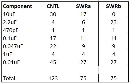
After reviewing the test results of the experiment, which showed good operation for all three of the groups, including the third group in which was considered to be a non-viable number of capacitors, we felt it was necessary to verify that each of the groups actually had the requested number of capacitors. We concluded that there had to be an error in how the three groups were assembled due to these unexpected results. So the production line engineers were asked to verify that each of the three groups had been correctly manufactured the way we had asked for in the Special Work Request (SWR). The configurations were verified. The test results had been so unexpected to us that it had to double-check. In this “aha” moment, we began to understand that the size and value of the capacitors – both large-valued voltage decoupling capacitors and small-valued noise decoupling capacitors – could be reduced further than we had predicted.
Conclusion
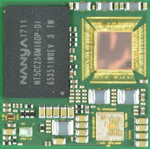
Although it would seem that reducing the number of passives has little to do with your design or any future design, but looking at Figure 3 we can see that the passives on the OSD3358-SM take up about 30% of the area or about 130 square millimeters. That is about the same area as the DDR in the upper left hand corner of the substrate. So the simple conclusion is by reducing the capacitors, not only does the cost go down, but the covered area by the passives goes down. This reduction in area can either be used to reduce the size of the SiP (e.g., reduce from 21mm to 18mm on a side), but the area could also be used for adding more components to it.
You can mark this down as one of the ways using SiP technology provides advantages that are not immediately visible.
Get More
Stay up to date on all of the latest innovations in System-in-Package. Sign up for the Octavo Systems newsletter.
"*" indicates required fields
