Develop the Smallest 1GHz Linux Edge Computing Platform with the AM335x Based OSD335x C-SiP
Published On: August, 6, 2019 By: Neeraj Dantu | Updated: January 29, 2020 by Greg Sheridan
This application note will provide a reference design to build a low cost 1GHz Linux Edge Computing Platform with AM335x Based OSD335x C-SiP. Both schematic and layout are discussed along with a demo sensor application. The board can be used for local processing and decision making as well as to send data to gateway/cloud through WiFi.

Get updates to the Linux Edge Computing Platform and all of the IoT Gateway projects
"*" indicates required fields
Table of Contents
1. Introduction
2. The Big Picture
3. Starting a Design with OSD335x C-SiP
4. Building the Schematic
4.1 Minimum Linux Boot Circuitry
4.1.1 Power and Ground Connections
4.1.2 Configuration Connections
4.1.3 AM335x – TPS65217C Connections
4.1.4 Boot Connections
4.2 Peripherals and I/O
4.2.1 USB
4.2.2 LEDs and Button
4.2.3 WiFi Module (Murata TYPE 1DX with CY4343W)
4.2.4 Light and Proximity Sensor
4.2.5 Pressure and Temperature Sensor
4.2.6 Inertial Motion Unit (IMU)
4.2.7 Expansion Header
5. Layout
5.1 Power and Ground Layout
5.2 USB Layout
5.3 WiFi Layout
5.4 Sensor Layout
5.5 Expansion Header Layout
6. Software Bring-Up
6.1 Base Linux Image
6.2 Bring-Up Sequence
6.3 WiFi Bring-Up
6.4 LED Bring-Up
6.5 Other Interfaces
6.6 Building and Setting Device Tree for Boot
6.7 Installing Sensor Libraries
6.7.1 VCNL4010 Library
6.7.2 BNO055 Library
6.7.3 BMP280 Library
7. Demo Application Using the Linux Edge Computing Platform
7.1 Environmental Sensing Application
7.2 Data Streaming Application
8. Conclusion
9.Revision History of this Document
![]()
![]() A PDF version of this App Note can be found HERE.
A PDF version of this App Note can be found HERE.
![]()
![]() Software files associated with this App Note can be downloaded HERE
Software files associated with this App Note can be downloaded HERE
![]()
![]() Design files associated with this App Note can be downloaded HERE.
Design files associated with this App Note can be downloaded HERE.
![]()
![]() A PDF version of the Schematics for this Reference Design can be found HERE.
A PDF version of the Schematics for this Reference Design can be found HERE.

1 Introduction
In recent years, as the IoT (Internet of Things) market has taken off, there has been an increased focus on edge computing. There are several advantages to having edge computing devices vs. stand-alone IoT sensors that only collect and report data to the cloud. The decentralized data processing approach used in edge computing not only limits the latency of decision making and can improve energy efficiency, but also “unclutters the cloud infrastructure” requiring only a fraction of the communication bandwidth. The OSD335x C-SiP is highly suitable for this application as it integrates a powerful 1GHz ARM Cortex™ A8 processor, power management, and enough RAM for local processing. Additionally, it has interfaces that connect to standard communication devices, such as , Bluetooth, and cellular modems, which allow data reporting/streaming to the cloud. In this application note, we will discuss how to easily design Linux Edge Computing Platform with the OSD335x C-SiP.
Before we dive into the design for the Linux Edge Computing Platform, the following links provide useful reference documentation that will help when designing a system with the OSD335x C-SiP:
- OSD335x C-SiP Design Tutorial:
https://octavosystems.com/app_notes/osd335x-c-sip-design-tutorial/
- OSD335x C-SiP Layout Guide:
https://octavosystems.com/app_notes/osd335x-c-sip-layout-guide/
- OSD335x C-SiP Power Application Note:
https://octavosystems.com/app_notes/osd335x-c-sip-power-application-note/
- OSD335x C-SiP Schematic Checklist:
https://octavosystems.com/app_notes/osd335x-schematic-checklist-am335x/
2 The Big Picture
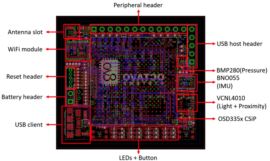
The hardware and software developed in this Linux Edge Computing Platform Application Note and Reference Design will be one piece of a larger project that demonstrates an IoT system using the OSD335x Family of devices. The IoT system employs a sensor-gateway-display architecture as seen in Figure 1. The hardware developed in this project will have 2 main functions to showcase the edge computing functionality of OSD335x C-SiP.
- Collect and process sensor data locally and make decisions based on the data
- Collect and transmit data to an IoT gateway to be processed, stored, and displayed remotely
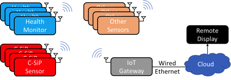
The documentation for the health monitor sensor shown in the IoT system has already been published and can be found at:
- Blog: https://octavosystems.com/2019/04/05/health-monitor-osd335x/
- io project: https://bbb.io/+1250bd
Additional application notes on the IoT Gateway and Remote Display will be published in the future.
3 Starting a Linux Edge Computing Platform Design with OSD335x C-SiP
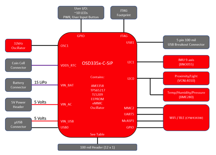
The first thing to do when starting any design is to create a block diagram of the design based on the requirements. The goal of this Linux Edge Computing Platform design is to collect data from some sensors and send the data to an IoT gateway over WiFi. Additionally, we would like to expose enough I/O to support an expansion board. The following requirements were formulated for the design:
- WiFi for connectivity
- IMU for orientation sensing
- Pressure sensing
- Light/proximity sensing
- USB client port
- Battery support
- RTC only mode with coin cell battery
- Expansion Interface
- USB host pins for additional connectivity
- GPIOs for additional programmability
Figure 2 shows the block diagram for the design, including the components and interface connections.
4 Building the Schematic
The next step is to build a schematic. The main steps for building a schematic with the OSD335x C-SiP are:
- Connect power and essential signals
- Add resistors for system boot configuration
- Add peripheral devices and I/O
The simplicity of this process comes from the amount of integration OSD335x C-SiP provides by including all the components required for a Linux boot. The following sections will discuss different parts of the schematic in detail.
4.1 Minimum Linux Boot Circuitry
The minimum circuitry needed to boot Linux includes the following:
- Power and Ground Connections
- Configuration Connections
- Required Connections between the TPS65217C and AM335x
- SYSBOOT Configuration
4.1.1 Power and Ground Connections
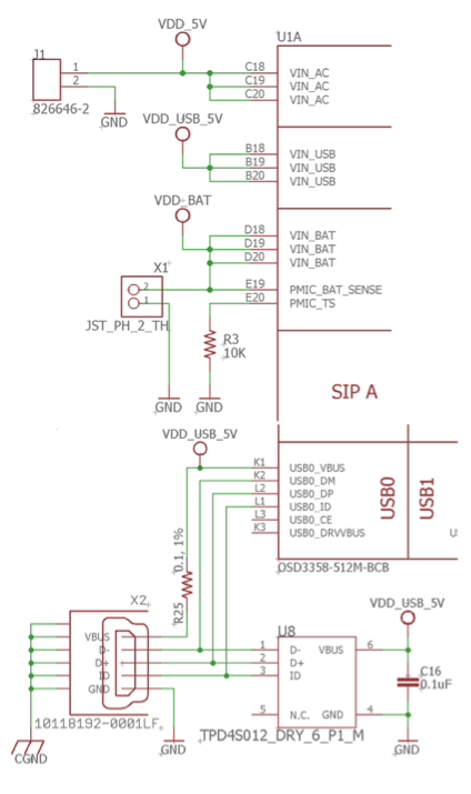
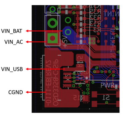
The OSD335x C-SiP has 3 power inputs, VIN_AC, VIN_USB and VIN_BAT. For this design, we can expose all three ways of powering the board with minimal effect on size of the board. The following figure shows a 100-mil header for VIN_AC, a 2-pin JST connector for VIN_BAT, and a USB client port for VIN_USB as seen in Figure 3. The C-SiP can be powered by any of these inputs and the power management integrated circuit (PMIC) within the OSD335x C-SiP will generate all of the necessary output power rails to power all the other components on the board as seen in Figure 4.
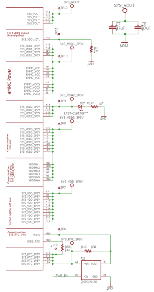
For the power outputs, there are connections that must be made as seen in Figure 4:
- From the datasheet, SYS_VOUT needs at least 50uF of capacitance (C7 and C8)
- To implement some low power modes, SYS_VDD1_CTL needs a weak pull down to ensure that SYS_VDD1_3P3V is off when the PMIC is in reset (R13)
- To signal the PMIC is powered on, an LED was added to SYS_VDD2_3P3V (D2)
- Given all I/O in the design is 3.3V, the VDDSHVx pins are connected to SYS_VDD3_3P3V
- To implement some low power modes while complying with power up sequencing, circuitry was added between VDDS and VDDS_RTC (U2)
4.1.2 Configuration Connections
In addition to the power and ground connections, we need circuitry for clocks, reset, and other configuration control inputs. Fortunately, the OSD335x C-SiP takes care of most of this. However, the design still needs a power button and a small header to make debug and bring-up easier.
Figure 5 shows the power button (S1) as well as the configuration header (J2) that contains both the processor and PMIC resets. Additionally, the configuration header contains the EEPROM write protect signal that must be grounded in order to program data into the EEPROM.
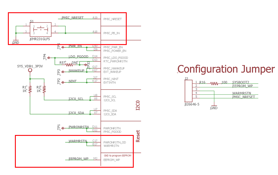
4.1.3 AM335X – TPS65217C Connections
Although both the TPS65217C PMIC and the AM335x processor are integrated with the OSD335x C-SiP, the connections between these devices are done externally to provide flexibility for power designs. For example, Section 7.5 of the OSD335x C-SiP datasheet shows different connection schemes needed to enable or disable the RTC subsystem. In this design, the RTC subsystem is enabled. Figure 6 shows the connections between the PMIC and the processor:
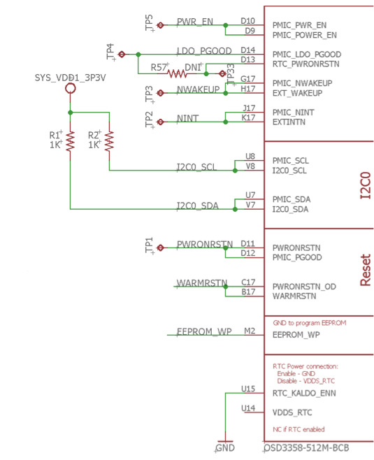
Additionally, we recommend adding test points for important signals to make bring-up and debug easier. From the schematic checklist, here are the signals that we recommend adding test points:
- Boot Signals: PMIC_POWER_EN, RTC_PWRONRSTN, EXT_WAKEUP, EXTINTN
- Reset/Control Signals: PWRONRSTN, WARMRSTN, PMIC_NRESET, SYS_VDD1_CTL
- Output Power Rails: SYS_VOUT, SYS_VDD1_3P3V, SYS_VDD2_3P3V, SYS_VDD3_3P3V, SYS_RTC_1P8V, SYS_VDD_1P8V
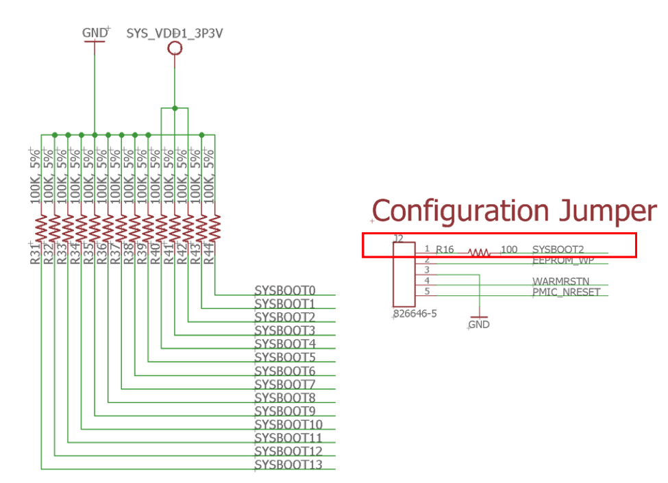
4.1.4 Boot Configuration
For this design, the intended boot peripherals are USB (USB0) and eMMC (MMC1). The OSD335x C-SiP will primarily boot from eMMC. However, having the ability to boot from USB makes it easy to bring-up the design and re-program the eMMC if there is a problem.
As seen in Figure 7, the boot configuration pins (i.e. SYSBOOT[13:0] which are pins LCD_DATA[13:0]) are set to 0x001C. The results in a boot peripheral order of MMC1, MMC0, UART0, USB0. When the eMMC is not programmed, this will allow the OSD335x C-SiP to boot from USB. When the eMMC is programmed, then the OSD335x C-SiP will always boot from the eMMC. However, to provide the ability to re-program the eMMC, the SYSBOOT2 (LCD_DATA2) pin is connected to a header which will cause the OSD335x C-SiP to bypass the eMMC on boot when connected to ground.
SYSBOOT[15:14] (LCD_DATA[15:14]) are set inside the OSD335x C-SiP to match the frequency of the integrated oscillator.
4.2 Peripherals and I/O
The following list of peripherals need to be added to the design:
- USB client port for USB0
- Expansion header for USB1
- User LEDs and a button for I/O
- WiFi Module
- Light & Proximity Sensor
- Pressure and Temperature Sensor
- 9 axis Inertial Motion Unit (IMU)
- Expansion header
4.2.1 USB
As seen in Figure 8, the USB0 interface is configured as a USB client and connected to a micro USB connector (X2). The USB1 interface is configured as a USB host and connected to a header (J4).
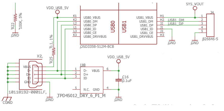
Power can be provided on the VBUS pin of X2 to power the device. Additionally, power is provided from the OSD335x C-SiP to the USB1 VBUS pin of J4 to serve as a power source for a peripheral device.
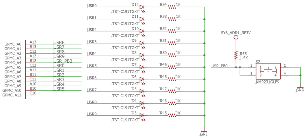
4.2.2 LEDs and Button
GPMC pins are chosen to be used as general purpose I/O for an LED array and the push button. Figure 9 shows the LEDs, push button and corresponding connections to OSD335x C-SiP
4.2.3 WiFi Module (Murata TYPE 1DX with CY4343W)
The TYPE 1DX module from Murata was chosen for this design because of its compact size and driver support within Linux. Please refer to the application note “Adding WiFi to Your Design: Cypress CY4343W + OSD335x” for more information on the hardware and software aspects of connecting the Murata module.
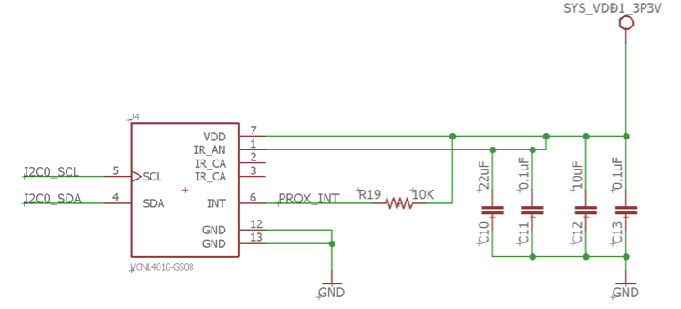
4.2.4 Light and Proximity Sensor
The Vishay VCNL4010 (https://www.vishay.com/docs/83462/vcnl4010.pdf) proximity and ambient light sensor was chosen for this design. This device has an I2C interface with the 7 bit address: 0x13. This device is powered using SYS_VDD1_3P3V and is placed on I2C0 interface. Figure 10 shows the schematic circuit for this device:
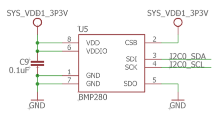
4.2.5 Pressure and Temperature Sensor
The Bosch BMP280 (https://ae-bst.resource.bosch.com/media/_tech/media/datasheets/BST-BMP280-DS001.pdf) pressure and temperature sensor was chosen for this design. This device has an I2C interface with the 7 bit address 0x76. This device is powered using SYS_VDD1_3P3V and is placed on the I2C0 interface. The following figure shows the schematic circuit for this device:
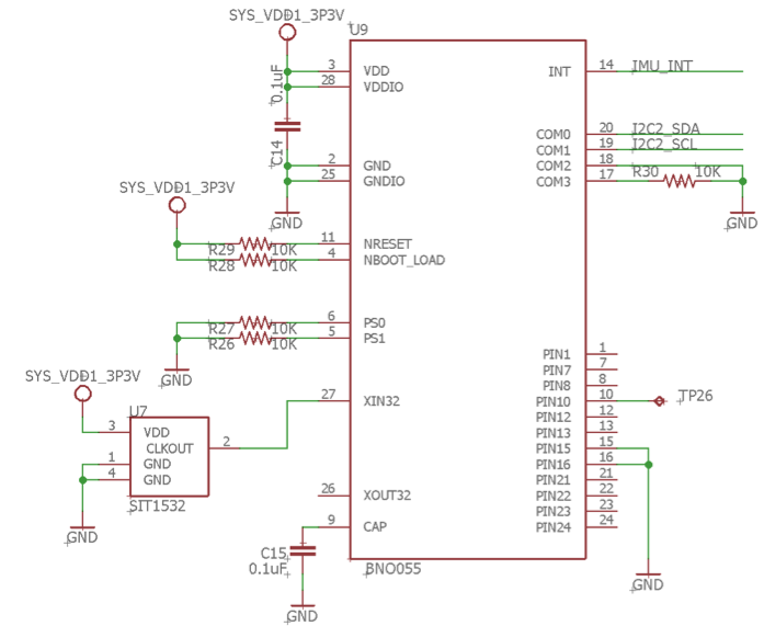
4.2.6 Inertial Motion Unit (IMU)
The Bosch BNO055 (https://ae-bst.resource.bosch.com/media/_tech/media/datasheets/BST-BNO055-DS000.pdf) with integrated gyroscope, accelerometer and geomagnetic sensor was chosen for this design. This device has an I2C interface with the 7 bit address 0x28. This device is powered using SYS_VDD1_3P3V and is placed on the I2C2 interface. Figure 12 shows the schematic circuit for this device:
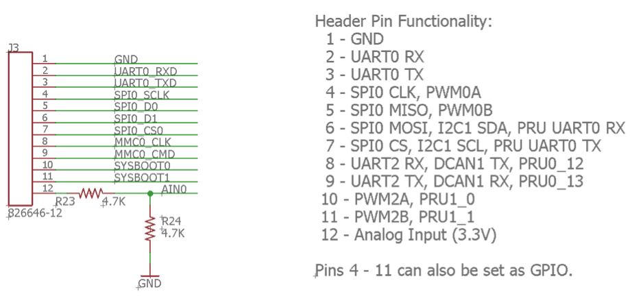
4.2.7 Expansion Header
A 12 pin 100 mil header is used to expose 12 I/O signals from OSD335x C-SiP. As discussed above, this allows for additional functionality to be added as well as provide debug capabilities in Linux. The header and functions of the 12 pins are shown in Figure 13.
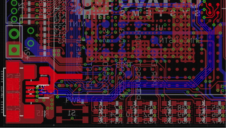
5 Layout
The goals for the layout are as follows:
- Single side placement with only optional components on the back
- 4 layer PCB with 2 signal layers and 2 power/ground plane layers
- 6 mil trace width and 6 mil spacing with 12 mil drill and 24 mil diameter via
- Design for testability and debug
With these goals in mind, the following layer organization is used:
- Top layer: Top side components + signal routing
- Layer 2: GND plane
- Layer 15: Power plane (SYS_VDD1_3P3V)
- Bottom layer: Optional bottom side components + signal routing
All the required components are placed on a single side of the PCB to reduce the cost of manufacturing. Components on the back are optional and would need to be populated by hand after manufacturing. After placing all the required components on the top layer, the size of this design came out to be 40mm x 35 mm. At 4cm x 3.5cm, this is one of the smallest single board computers that integrates a 1GHz processor, 512MB of RAM and on board WiFi. The finished layout is shown in Figure 14.
The following sections describe different aspects of the layout.
5.1 Power and Ground Layout
The power and ground planes are designed to act as a reference as well as provide connections where necessary. All three power input methods, VIN_AC, VIN_USB and VIN_BAT, are available to power this design as seen in Figure 15.
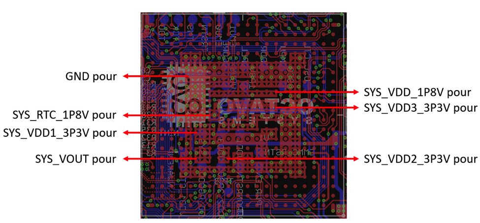
Copper pours are created to connect the 3 inputs with corresponding headers. Copper pours are also added the power and ground rails of the processor as seen in Figure 16. Multiple vias are used to increase electrical and thermal performance of the design. The ground (GND) pour is connected to the GND plane (Layer 2) and the SYS_VDD1_3P3V pour is connected to the power plane (Layer 15).
5.2 USB Layout
The USB client layout is highlighted in Figure 17.
The USB0_DP and USB0_DM signals are high speed data signals and need to be length and impedance matched.
The USB host header is highlighted in Figure 18. As with the client port, USB1_DP and USB1_DM are length and impedance matched. The SYS_OUT power rail supplies the up to 500 mA of power for any device connected to this header which requires a larger power trace.
5.3 WiFi Layout
Please refer to the application note “Adding WiFi to Your Design: Cypress CY4343W + OSD335x” for more information on the layout aspects of connecting the Murata module.
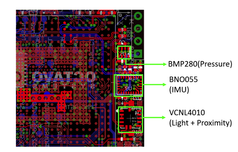
5.4 Sensor Layout
Figure 19 highlights the layout for the sensors integrated in the design. All three sensors are connected to the I2C0 data bus. Power is provided by the SYS_VDD1_3P3V power plane for each of the devices.
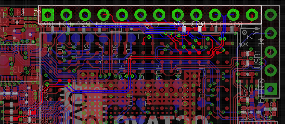
5.5 Expansion Header Layout
The 12 pin 100 mil spaced header used to expose some GPIO interfaces is highlighted in Figure 20.
6 Software Bring-Up
To begin developing an application with this Linux Edge Computing Platform, it is necessary to enable all the device drivers for the devices on board. This section describes the bring-up and initialization process for the design.
6.1 Base Linux Image
Because the board utilizes an OSD335x System in Package family member based on the Sitara® AM335x ARM® Cortex® A8 processor from TI, there are many Linux distributions available. As a starting point for development, we encourage developers to look at the open source Linux image from BeagleBoard.org®. BeagleBoard.org® , a customer of Octavo Systems, has several SBC boards that are excellent examples of using an OSD335x SiP in a design. BeagleBoard.org® has developed a strong and vibrant community around their families of boards.
The latest software images are available at http://beagleboard.org/latest-images. A Debian 9.5 IoT image was used as the base for the software development in this project.
6.2 Bring-Up Sequence
There are several devices in the design that need to be initialized to be used in an application. The following steps describe the sequence to initialize each of these devices:
- Bring-up WiFi Interface
- Bring-up the controls for the LEDs
- Initialize the communication interfaces that allow the processor to communicate with the sensors and external devices
- Bring-up application programming interfaces for each sensor
The first 3 steps can be accomplished in the device tree. However, when interfacing with a sensor, it is important to understand both the kernel drivers and open source user space libraries that are available. Depending on the features provided by the drivers and libraries, you can decide how to interact with the sensor from an application perspective.
The following files available in this application note download folder are used in the bring-up process:
- osd335x-csip.dtsi: This is a device tree source include file that described the hardware integrated in OSD335x CSiP
- dts: This device tree source file describes the WiFi, USB and other I/O multiplexing for the kernel hardware initialization
If you are unfamiliar with device trees or need a quick refresher, please take a look at the application note “OSD335x Lesson 2: Linux Device Tree”.
6.3 WiFi Bring-Up
Please refer to the application note “Adding WiFi to Your Design: Cypress CY4343W + OSD335x” for more information on the software bring-up aspects of connecting to the Murata module.
6.4 LED Bring-Up
There are two sections that need to be added in the Device Tree in order to configure the kernel for user space interaction with LEDs.
- Setup the pin multiplexing (pinmux) for the LED pins
- Declare these pins as LEDs
The following snippet of the Device Tree shows the pinmux for the LEDs:
1 2 3 4 5 6 7 8 9 10 11 12 13 14 15 16 17 | &am33xx_pinmux { user_leds_s0: user_leds_s0 { pinctrl-single,pins = < AM33XX_IOPAD(0x840, PIN_OUTPUT_PULLDOWN | MUX_MODE7) /* gpmc_a0.gpio1_16 */ AM33XX_IOPAD(0x844, PIN_OUTPUT_PULLDOWN | MUX_MODE7) /* gpmc_a1.gpio1_17 */ AM33XX_IOPAD(0x848, PIN_OUTPUT_PULLDOWN | MUX_MODE7) /* gpmc_a2.gpio1_18 */ AM33XX_IOPAD(0x84c, PIN_OUTPUT_PULLDOWN | MUX_MODE7) /* gpmc_a3.gpio1_19 */ AM33XX_IOPAD(0x854, PIN_OUTPUT_PULLDOWN | MUX_MODE7) /* gpmc_a5.gpio1_21 */ AM33XX_IOPAD(0x858, PIN_OUTPUT_PULLDOWN | MUX_MODE7) /* gpmc_a6.gpio1_22 */ AM33XX_IOPAD(0x85c, PIN_OUTPUT_PULLDOWN | MUX_MODE7) /* gpmc_a7.gpio1_23 */ AM33XX_IOPAD(0x860, PIN_OUTPUT_PULLDOWN | MUX_MODE7) /* gpmc_a8.gpio1_24 */ AM33XX_IOPAD(0x864, PIN_OUTPUT_PULLDOWN | MUX_MODE7) /* gpmc_a9.gpio1_25 */ AM33XX_IOPAD(0x868, PIN_OUTPUT_PULLDOWN | MUX_MODE7) /* gpmc_a10.gpio1_26 */ AM33XX_IOPAD(0x850, PIN_INPUT_PULLUP | MUX_MODE7) /* gpmc_a10.gpio1_26 */ >; }; }; |
The next snippet, shows how to set up the LEDs connection to the corresponding GPIO pin, default state, triggers and label them as ‘usrX’ within node ‘leds’.
1 2 3 4 5 6 7 8 9 10 11 12 13 14 15 16 17 18 19 20 21 22 23 24 25 26 27 28 29 30 31 32 33 34 | leds { pinctrl-names = "default"; pinctrl-0 = <&user_leds_s0>; compatible = "gpio-leds"; led2 { label = "usr0"; gpios = <&gpio1 21 GPIO_ACTIVE_HIGH>; linux,default-trigger = "heartbeat"; default-state = "off"; }; led3 { label = "usr1"; gpios = <&gpio1 22 GPIO_ACTIVE_HIGH>; linux,default-trigger = "mmc0"; default-state = "off"; }; <OTHER LED LABELS NOT SHOWN> led10 { label = "usr8"; gpios = <&gpio1 18 GPIO_ACTIVE_HIGH>; default-state = "off"; }; led11 { label = "usr9"; gpios = <&gpio1 19 GPIO_ACTIVE_HIGH>; default-state = "off"; }; }; |
6.5 Other Interfaces
Within the Device Tree, a few other nodes initialize I2C (I2C0, I2C2), USB (host and client), UART (UART0 for Linux console) and MMC (eMMC). Please refer to the project device tree files for this information. The sensors on this board reside on the I2C0 and I2C2 interfaces. To use kernel drivers for these sensors, we would configure this in the i2c0 node and the i2c2 node of the device tree. However, for this project, we will use user space libraries, so the interfaces only need to be enabled.
6.6 Building and Setting Device Tree for Boot
Building the Device Tree and setting the Device Tree for Linux boot is described in the OSD335x Device Tree tutorial: https://octavosystems.com/app_notes/osd335x-design-tutorial/osd335x-lesson-2-minimal-linux-boot/linux-device-tree/
6.7 Installing Sensor Libraries
For this project, we will use Python libraries to interact with the sensors instead of using kernel drivers. These Python libraries provide an easy to use API for accessing the sensors. All three libraries use ‘smbus’ Python package. The package can be installed by using the following instruction:
1 | $ sudo pip install smbus |
6.7.1 VCNL4010 Library
Execute the following instructions to install the “Adafruit_Python_VCNL40xx” library:
1 2 3 | $ git clone https://github.com/adafruit/Adafruit_Python_VCNL40xx $ cd Adafruit_Python_VCNL40xx/ $ sudo python setup.py install |
6.7.2 BNO055 Library
Execute the following instructions to install the “Adafruit_Python_BNO055” library:
1 2 3 | $ git clone https://github.com/adafruit/Adafruit_Python_BNO055 $ cd Adafruit_Python_BNO055/ $ sudo python setup.py install |
6.7.3 BMP280 Library
Execute the following instructions to install the “bmp280-python” library:
1 2 3 | $ git clone https://github.com/pimoroni/bmp280-python $ cd bmp280-python/ $ sudo ./install.sh |
7 Demo Application Using the Linux Edge Computing Platform
The demo application for this project will demonstrate how to perform local processing of data and send a data stream to a IoT gateway over WiFi. This will be done in two separate applications:
- Environment Sensing: BMP280 temperature and pressure data is read, analyzed and LEDs are set based on the information.
- Data Streaming: Orientation data from BNO055 and Proximity + ambient light data from VCNL4010 are streamed to an IoT gateway via WiFi.
7.1 Environmental Sensing Application
The file env_sense.py found in the application note download folder performs environmental sensing. The code uses the bmp280-python library to check the current temperature and pressure reading and compares them to a predefined range of values. If the temperature and pressure values are out of the predefined range, an LED is activated.
Execute the following command to run the application as a background process:
1 | $ sudo python env_sense.py & |
7.2 Data Streaming Application
The file data_stream.py in the application note download folder performs data streaming. The application reads orientation data, ambient light, and proximity data and sends them to an IoT gateway using a separate sensor gateway application.
Before running data_stream.py, the sensor_gateway application which can be found in the application note download folder needs to be installed. The sensor_gateway application creates a command line interface to transfer data from a client sensor to an IoT Gateway. Execute the following commands to unzip and build the executable:
1 2 3 | $ unzip sensor_gateway.zip $ cd sensor_gateway $ make |
The executable msg_client will be used to stream data to the gateway.
Before executing the streaming application, the path to msg_client must be updated in data_stream.py. This path must be assigned to the variable ‘MSG_CLIENT’ which by default is ‘/var/lib/cloud9/gw_demo/msg_client’, meaning that sensor_gateway application was downloaded and unzipped in ‘/var/lib/cloud9/’.
1 | $ sudo python data_stream.py |
Execute the following command to run the data streaming application:
1 2 | $ sudo python env_sense.py & $ sudo python data_stream.py |
An example output of data_stream.py is shown below:
1 2 3 4 5 6 7 8 9 10 | Starting C-SiP sensor | Proximity | Ambient | Heading | Roll | Pitch | |------------|-------------|----------|-------------|-------------| | 2094 | 679 | 350.06 | 28.62 | -34.00 | | 2093 | 677 | 350.00 | 28.62 | -34.00 | | 2095 | 679 | 349.94 | 28.94 | -34.62 | | 2098 | 682 | 349.81 | 29.31 | -35.25 | . . . |
8 Conclusion
This project shows how easy it is to prototype an IoT measurement system and Linux Edge Computing Platform by using the low cost and easy to use OSD335x Family of System in Package devices. The hardware integration and availability of opensource software make the OSD335x Family of devices and in particular the OSD335x CSiP a uniquely suited device for IoT and Linux Edge Computing Platforms.
9 Revision History
| Revision Number | Revision Date | Changes | Author |
|---|---|---|---|
| 1 | 8/06/2019 | Initial Release | N. Dantu |
