Adding WiFi to Your Design: Cypress CY4343W + OSD335x
Published On: July, 26, 2019 By: Neeraj Dantu | Updated: August 13, 2019 by Cathleen Wicks
This application note describes the procedure to connect the Cypress Semiconductor CY4343W WiFi/BLE module to the the OSD335x, the AM335x System in Package, Family of Devices . It will walk through both hardware design as well as software integration within Linux. For this application note, the OSD335x C-SiP is used as an example for implementation of the hardware and software. However, the same logical hardware design can be used for the other devices in the OSD335x Family of devices, such as the OSD335x and OSD335x-SM.
The CY4343W (https://www.cypress.com/file/298081/download) from Cypress Semiconductor is a single chip 802.11 b/g/n WiFi module that also supports Bluetooth 4.1. The data connection for the WiFi module is a standard SDIO v2.0 interface. The CY4343W is integrated within the Type 1DX module (https://wireless.murata.com/type-1dx.html) from Murata. This module provides the necessary clocks and passive components around the CY4343W and comes as an ultra-small 6.95 mm x 5.15 mm x 1.1 mm LGA package. This makes it possible to easily add WiFi to an embedded design while still having a compact form factor.
The application note is organized as follows: Section 2 describes the schematic connections between the OSD335x C-SiP and 1DX module as well as the layout considerations when placing these components on a printed circuit board (PCB). Section 3 describes enabling communication between OSD335x C-SiP and 1DX module in software by adding the necessary device tree entries and configuring and loading the appropriate Linux drivers.
This application note only covers communication with the WiFi interface of the 1DX module. Bluetooth/PCM are not included at this time.
Get updates to this application note and all of our technical documentation.
"*" indicates required fields
Table of Contents
1.Introduction
2. Connecting the CY4343W Module to the OSD335x
2.1 Power
2.2 Communication Interfaces
2.2.1 SDIO Interfaces
2.3 Layout
2.3.1 Power
2.3.2 Noise Reduction
2.3.3 Interface Routing
2.3.4 Antenna Routing
3. Enabling the WiFi Module
3.1 Creating the Device Tree
3.1.1 Enabling the MMC Interface
3.1.2 Setting the Pin Multiplexing
3.1.3 Enabling the Module
3.1.4 Building the Device Tree
3.2 Copy NVRAM Text File
3.3 Update and Load brcmfmac Kernel Module
3.3.1 Building Your Own Kernel
3.3.2 Using a Pre-built Linux Image
3.3.3 Verification
4. Conclusion
5.Revision History of this Document
![]()
![]() A PDF version of this App Note can be found HERE
A PDF version of this App Note can be found HERE
![]()
![]() Files associated with this App Note can be downloaded HERE
Files associated with this App Note can be downloaded HERE

2 Connecting the CY4343W Module to the OSD335x
Figure 1 shows a high-level block diagram of the 1DX module:
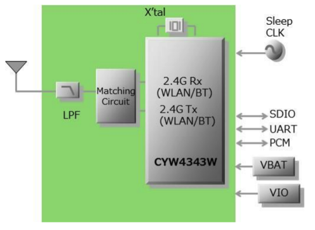
The VIO and VBAT inputs are used to power the module. For communication with the OSD335x, the module uses the SDIO interface for WiFi, the UART interface for Bluetooth, and a PCM interface for Bluetooth audio.
2.1 Power
The CY4343W 1DX module has two power inputs with additional voltages being provided by the regulators inside CY4343W. VBAT is the main DC supply input with an operating voltage range of 3V – 4.8V. For optimal performance, the datasheet for CY4343W recommends powering the module with a DC voltage between 3.2V and 4.8V. The DC supply voltage for the I/O (VIO) can be between 1.71V and 3.63V. So, both 1.8V and 3.3V I/O is possible. Figure 2 shows a configuration in which 3.3V is used to supply power to both VBAT and VIO. In addition, the internal regulator output SR_VLX is connected to the internal 1.35V LDO input VIN_LDO via an inductor.
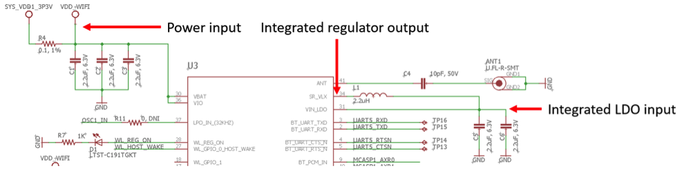
The maximum current consumption of the module is listed as 370mA for WiFi and 60mA for Bluetooth. So, a 3.3V power supply rail with sufficient current capacity needs to be selected to power the module. The OSD335x integrates a 3.3V LDO that can supply up to 500mA (i.e. SYS_VDD1_3P3V). Therefore, this power rail can be used to power the module. A power isolation resistor(R4) is used to isolate the power input of the module from the OSD335x power output rail. This resistor can be replaced with noise filtering inductor if needed.
2.2 Communication Interfaces
The CY4343W 1DX module provides a 4-bit SDIO interface for WiFi communication, a UART interface for Bluetooth communication, and a PCM interface for Bluetooth audio communication. These interfaces along with the corresponding control signals need to be connected to the communication interfaces and I/O of OSD335x. In this application note, we will only discuss the WiFi interfacing.
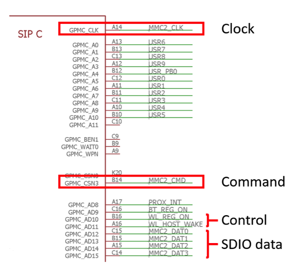
2.2.1 SDIO Interface
The SDIO interface is an extension of the SD interface commonly found on microSD cards and is closely related to the MMC (Multi-Media Card) interface. The AM335x processor within the OSD335x contains three MMC peripherals that support both MMC and SDIO communication. So, the SDIO slave interface of the module can be connected to the MMC interface of the OSD335x as see in Figure 4. The SDIO interface consists of a command signal (SDIO_CMD), a clock signal (SDIO_CLK), and up to 4 data signals (SDIO_DATA_x). The command signal is used by the host to send commands and receive responses from the slave device while the data signals are used to transfer data based on the command. Both the command and data signals are synchronized by the clock generated by the host. The interface typically runs about 50MHz. The CY4343W uses a 4-bit SDIO version 2.0 interface.
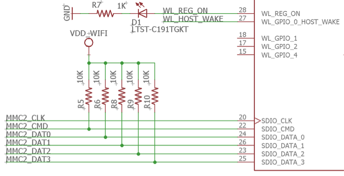
The WL_REG_ON and WL_HOST_WAKE signals in Figure 4 are control signals for the wireless module that should be connected to the OSD335x. When WL_REG_ON is high, all the internal regulators of the CY4343W are enabled and the WiFi section of the device is out of reset. This pin has an internal pull-down resistor that puts the WiFi in reset by default. WL_HOST_WAKE is a GPIO pin that can be used to wake the OSD335x up from low power states when the CYC4343W receives WiFi communications.
Figure 5 shows the SDIO interface signals connected to the MMC2 interface of the OSD335x. The WL_REG_ON and WL_HOST_WAKE signals are connected to GPIO pins that can be configured in the device tree.
2.3 Layout
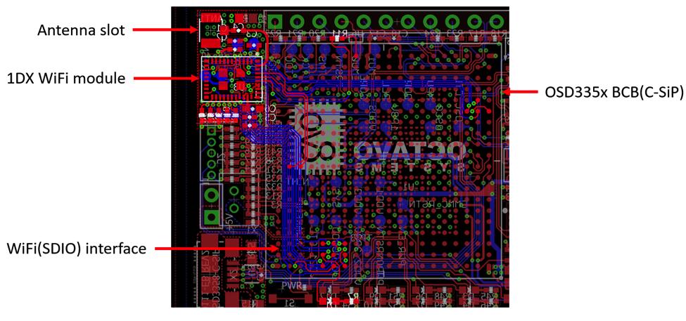
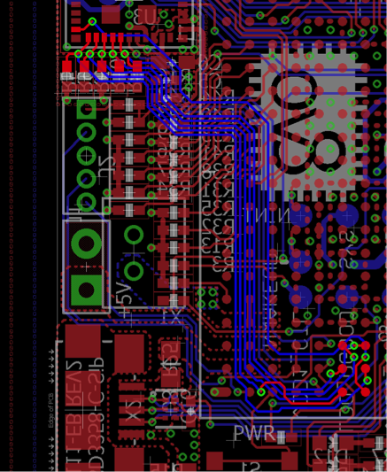
Figure 6 shows the layout for CY4343W 1DX module connected to the OSD335x C-SiP.
2.3.1 Power
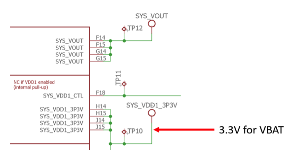
The power for the CY4343W 1DX module is supplied by the SYS_VDD1_3P3V internal LDO of the OSD335x C-SiP. The power layout is highlighted in Figure 7:
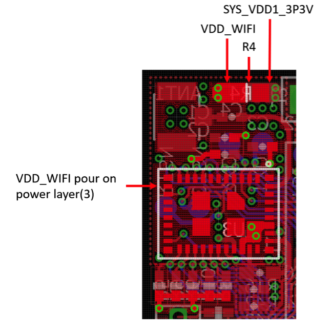
Small copper pours are used to connect either side of the 0805 power isolation resister R4 to SYS_VDD_3P3V and VDD_WIFI. All the power pins are connected to the power rail VDD_WIFI through vias. Thick (~10mil) traces are used for higher current carrying capacity. All the ground pins are connected to the GND plane through vias. In this design the GND plane is layer 2.
2.3.2 Noise Reduction
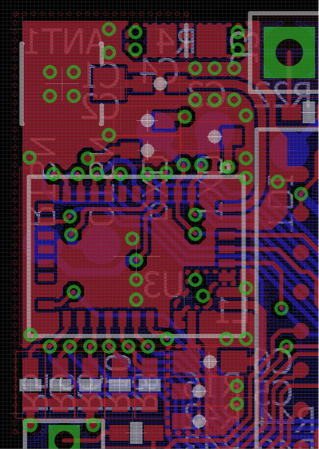
To help reduce the noise around the CY4343W 1DX module, the top layer is flooded with a copper ground pour as seen in Figure 8. This pour is connected to the ground layer wherever possible with vias.
2.3.3 Interface Routing
The SDIO interface runs at 50MHz. So, best practices for signal integrity should be followed for traces of SDIO (MMC2) signals CLK, CMD, D0, D1, D2 and D3. There is some leeway when it comes to length matching as the interface speed is not as high as say Ethernet. The following figure shows an example of the SDIO interface routing.
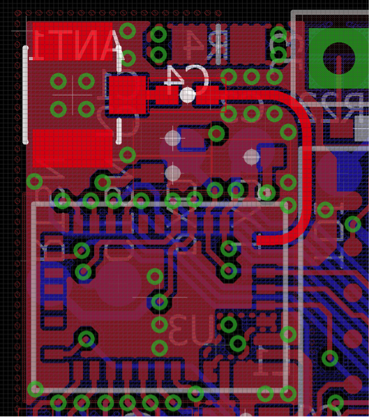
2.3.4 Antenna Routing
The signal using the trace that feeds the RF antenna connector from the CY4343W 1DX module runs at approximately 2.4GHz. Therefore, it must be routed with great care to ensure good RF performance. The placement of the module needs to be such that the antenna trace is close to the edge of the PCB to isolate it from other signals. Additionally, the RF trace is as short as possible with an appropriate ground reference underneath the routing layer. Via stitching around the RF trace between the copper ground pour on the top layer of the printed circuit board and the ground plane is done to also help minimize noise. Because of the speed of the signal, mitered traces should be used to gradually change directions versus the typical 135 degree bend found in lower speed traces. Also, the RF trace should have constant 50 ohm impedance to match the antenna connector to minimize the reflections caused by an impedance mismatch. Filter circuitry is also included on the trace to help mitigate impedance mismatches. Figure 10 shows the antenna trace connected to the antenna connector in layout.
3 Enabling the WiFi Module
Bringing up the CY4343W 1DX WiFi module requires the following steps:
- Create a Device Tree with proper entries and generate the Device Tree Binary
- Copy the NVRAM text file to the appropriate directory to initialize the module
- Update and load the brcmfmac kernel module
The following sections will walk through the detailed procedures required to complete these steps.
3.1 Creating the Device Tree
For the Linux kernel to identify the CY4343W 1DX module and load the appropriate kernel modules, it needs proper Device Tree entries. If you are unfamiliar with Device Trees or need a quick refresher, please look at the following resources:
- OSD335x Device Tree Tutorial: https://octavosystems.com/app_notes/osd335x-design-tutorial/osd335x-lesson-2-minimal-linux-boot/linux-device-tree/
- OSD335x Linux Boot Process: https://octavosystems.com/app_notes/osd335x-design-tutorial/osd335x-lesson-2-minimal-linux-boot/osd335x-lesson-2-linux-boot-process-with-the-osd335x/
For this application note, we have modified Device Tree Source files which are available in the download folder for this application note. We have provided two files, but all modifications have occurred only in the second file:
- osd335x-csip.dtsi: Device Tree source include file for the OSD335x C-SiP
- dts: Device Tree source file describing the WiFi module interface with OSD335x C-SiP.
The following code snippets show the parts of the Device Tree that have been edited to enable the CY4343W 1DX module during the Linux boot of the OSD335x C-SiP.
3.1.1 Enabling the MMC Interface
In the example implementation seen in Figure 5, the CY4343W 1DX module is connected to the MMC2 interface. This requires that the mmc3 device tree node be updated edited in Device Tree due to a zero indexing versus one indexing mismatch between the hardware peripheral name and the device tree node.
1 2 3 4 5 6 7 8 9 10 11 12 13 14 15 16 17 18 19 20 21 22 23 | &mmc3 { #address-cells = <1>; #size-cells = <0>; pinctrl-names = "default"; pinctrl-0 = <&mmc3_pins>; vmmc-supply = <&wlan_en_reg>; max-frequency = <20000000>; bus-width = <0x4>; ti,non-removable; ti,needs-special-hs-handling; // cap-power-off-card; keep-power-in-suspend; status = "okay"; brcmf: wifi@1 { reg = <1>; compatible = "brcm,bcm4329-fmac"; interrupt-parent = <&gpio0>; interrupts = <27 GPIO_ACTIVE_HIGH>; interrupt-names = "host-wake"; brcm,overclock-50 = <20>; }; }; |
As you can see in this snippet, the pin multiplexing node, mmc3_pins, and enable node, wlan_en_reg, are set (see below for more code details). Additionally, the SDIO bus width is set to 4-bits, the maximum bus operating frequency is set to 20MHz to avoid any clock related errors, and the WL_HOST_WAKE interrupt is connected to the appropriate GPIO pin based on the schematic connections. Additionally, brcmf node is used to invoke the CY4343W Linux driver and provide the parameters required by the driver.
3.1.2 Setting the Pin Multiplexing
To communicate with the CY4343W 1DX module, we must set the pin multiplexing of the OSD335x C-SiP. This is done in the am33xx_pinmux node.
1 2 3 4 5 6 7 8 9 10 11 12 13 | // WiFi Module mmc3_pins: pinmux_mmc3_pins { pinctrl-single,pins = < AM33XX_IOPAD(0x9e4, PIN_OUTPUT_PULLUP | MUX_MODE7 AM33XX_IOPAD(0x82c, PIN_INPUT | MUX_MODE7) AM33XX_IOPAD(0x88c, PIN_INPUT_PULLUP | MUX_MODE3) AM33XX_IOPAD(0x888, PIN_INPUT_PULLUP | MUX_MODE3) AM33XX_IOPAD(0x830, PIN_INPUT_PULLUP | MUX_MODE3) AM33XX_IOPAD(0x834, PIN_INPUT_PULLUP | MUX_MODE3) AM33XX_IOPAD(0x838, PIN_INPUT_PULLUP | MUX_MODE3) AM33XX_IOPAD(0x83c, PIN_INPUT_PULLUP | MUX_MODE3) >; }; |
In this snippet, the first two lines show the pin multiplexing setup for the WiFi control signals WL_REG_ON and WL_HOST_WAKE while the other lines set up the MMC2 interface signals based on the connections in Figure 5. The hexadecimal numbers are address offsets within the AM335x control module which correspond to the control register for the given pin of the AM335x. You can find this information in the Technical Reference Manual for the AM335x(https://www.ti.com/lit/ug/spruh73p/spruh73p.pdf).
3.1.3 Enabling the Module
To enable the CY4343W 1DX module after power up, we need to add a regulator Device Tree node.
1 2 3 4 5 6 7 8 9 10 11 | wlan_en_reg: fixedregulator@2 { compatible = "regulator-fixed"; regulator-name = "wlan-en-regulator"; regulator-min-microvolt = <3300000>; regulator-max-microvolt = <3300000>; startup-delay-us= <70000>; /* WL_EN */ gpio = <&gpio3 7 0>; enable-active-high; }; |
In this snippet, the WL_HOST_EN signal is declared as GPIO bank 3 bit 7 which can be found in the schematic connection shown in Figure 5.
3.1.4 Building the Device Tree
To build the device tree, we will use the Device Tree Re-builder (dtb_rebuilder) provided by Robert Nelson. While this can be used on any Linux computer, it can also be used on an OSD3335x based development board with an internet connection.
The high-level procedure is as follows:
- Place osd335x-csip.dtsi and dts in a directory
- Clone the dtb-rebuilder
- Copy the device tree source files to the src/arm directory of the dtb-rebuilder
- Use make to build the device tree binary
1 2 3 4 5 6 | $ git clone https://github.com/RobertCNelson/dtb-rebuilder $ cp osd335x-csip.dtsi dtb-rebuilder/src/arm/ $ cp osd335x_wifi_example.dts dtb-rebuilder/src/arm/ $ cd dtb-rebuilder $ sudo make clean $ sudo make all |
The Device Tree binary output file osd335x_wifi_example.dtb will be generated in the dtb-rebuilder/src/arm directory. To use this file on a design, you will need to:
- Copy the dtb file to the /boot/dtbs/[kernel version] directory
- Modify the /boot/uEnv.txt file
- Change the #dtb= line to dtb=osd335x_wifi_example.dtb
3.2 Copy NVRAM Text File
During the initialization process of the CY4343W 1DX module, the chip name and version needs to be verified. Additionally, parameters need to be set within the module. To accomplish this, a text configuration file with the initialization parameters named brcmfmac43430-sdio.txt needs to be placed in /lib/firmware/brcm directory. This directory also contains firmware that will be loaded to the module during initialization.
An example configuration file is available in the application note download folder. This file needs to be placed in the /lib/firmware/brcm folder.
The module also requires a firmware file named brcmfmac43430-sdio.bin which must be in the /lib/firmware/brcm folder. This file is normally available as an option to be included in the root file system during the kernel build process. If it is not present, an example firmware in included in the above download folder.
3.3 Update and Load brcmfmac Kernel Module
By default, the kernel module invoked by the Device Tree is not compatible with the AM335x MMC driver. This leads to an error in the initialization process resulting in a failure to create the wireless network interface.
Depending on how you are building your embedded Linux software image, there are two methods to fix the driver and initiate the module correctly.
3.3.1 Building Your Own Kernel
If you are building your own kernel, a patch must be applied to the brcmfmac driver for the driver to work correctly. The modification is described in this forum thread:
https://e2e.ti.com/support/processors/f/791/t/541016?AM335X-Error-message-in-SDIO-driver
As seen from this thread, we must modify the drivers/net/wireless/broadcom/brcm80211/brcmfmac/common.c file to correct the misalignment of blocks between the OSD335x and CY4343W 1DX module.
3.3.2 Using a Pre-Built Linux Image
If you are using a pre-built Linux Image and are not rebuilding your kernel, you can instead update the kernel module binaries for the brcmfmac with the pre-built kernel modules in the application note download folder. The provided kernel modules are built for 4.14.x kernel. If you are using a different kernel version, the modules may work. However, if they do not after testing, it will be necessary to rebuild the kernel module with the patch described in Section 3.3.1.
To replace the kernel module, the following high-level procedure should be followed:
- Copy ko.xz to the target system
- Copy the brcmfmac43430-sdio.txt and brcmfmac43430-sdio.bin to target file system as described in section 3.2
- Reboot the board
To replace the current kernel module with the updated kernel module copy the kernel
module to the target system and then place it in the correct directory:
1 | sudo cp brcmfmac.ko.xz /lib/modules/[kernel version]/kernel/drivers/net/wireless/broadcomm/brcm/brcmfamc |
The [kernel version] needs to be replaced with the appropriate kernel version on the target system.
A second method is to insert the kernel module on the currently running system. First, we will need to remove the current kernel module and insert the new kernel module using the following commands:
1 2 | sudo rmmod brcmfmac sudo insmod brcmfmac.ko.xz |
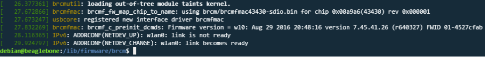
3.3.3 Verification
To check if the kernel module has been loaded correctly, you can check the dmesg output as shown in the screen capture:
4 Conclusion
This application note describes connecting the CY4343W 1DX module with the OSD335x Family of devices. If you have any questions or comments, please post on our forums.
5 Revision History
| Revision Number | Revision Date | Changes | Author |
|---|---|---|---|
| 1 | 7/25/2019 | Initial Release | N. Dantu |
