OSD32MP15x Schematic Checklist
Published On: August, 27, 2020 By: Eshtaartha Basu | Updated: January 28, 2021 by Greg Sheridan
Introduction
This application note provides a checklist to help users review schematics built around the OSD32MP15x, the STM32MP1x System in Package, Family of Devices. Going through this schematic checklist before or during the schematic design phase will help avoid common pitfalls. This OSD32MP15x schematic checklist targets a generic embedded system and is not exhaustive. Each design is unique, and your custom design may require additional in-depth verification to validate its overall functionality. Octavo Systems offers a Hardware Design Review Service to help with this in-depth verification.
The first section of this document consists of multiple checklists to help you validate each sub-section of your design. The second section (i.e., Appendix) consists of supplemental information to further aid your design validation. To get started, here are the top ten checklist questions and where answers can be found:
| ITEM | SECTION | SCHEMATIC CHECKLIST TOPIC | |
| ✓ | 1 | 2.1 | Prepared to Check your Power Design? |
| ✓ | 2 | 2.2 | Adding an Oscillator? |
| ✓ | 3 | 2.2 | Ready to Reset? |
| ✓ | 4 | 2.3 | Best Boot Configuration Settings? Make sure your design can boot properly. |
| ✓ | 5 | 2.4 & 2.6 | Planning for Peripheral Success? Check your USB, I2C, UART, SPI and more in this section. |
| ✓ | 6 | 2.6 | Prepping for Pinmux? Leaving off some peripherals? Let’s check your IO in this section. |
| ✓ | 7 | 2.5 | Enabling eMMC? Need non-volatile storage? Are meeting the requirements? |
| ✓ | 8 | 2.6 | Ready to Juggle JTAG? Check for a properly connected JTAG to be a great debug resource. |
| ✓ | 9 | 2.6 | Excited about EEPROM? Let’s check your EEPROM WP pin. |
| ✓ | 10 | 3.5 | Talk to out Team? |

Table of Contents
OSD32MP15x Schematic Checklist
Essential Connections and Power Design
| Topic No. | OSD32MP15x | SCHEMATIC CHECKLIST TOPIC – Mandatory | |
| PD1 | ✓ | Input Power Connections: Choose a power input use case from the Power Input Table based on design requirements and implement mandatory connections | |
| PD2 | ✓ | In-Rush Current: The power source connected to a power input must be able to supply the necessary in-rush current: ~0.25A for VIN | |
| PD3 | ✓ | External Capacitance: See the Passives Section and the Recommended Capacitors Table of the OSD32MP15x datasheet. | |
| PD4 | ✓ | IO Voltage: OSD32MP1 supports both 1.8V and 3.3V I/O (Default: 3.3V I/O). For 1.8V I/O, set output voltage of BUCK3 (which supplies VDD power domain) to 1.8V. In addition, see Figure 31 and 32 of Getting Started with STM32MP1 Hardware Development app note and STPMIC1 Non-Volatile Memory Programming Guide. | |
| PD5 | ✓ | Processor – PMIC Connections: All mandatory connections are done within the OSD32MP15x SiP. See section 7.2 of OSD32MP15x datasheet for more info. | |
| PD6 | ✓ | VBAT Operation/RTC/backup registers/retention RAM(1): Choose one of the use cases from the VBAT table. | |
| PD7 | ✓ | VDD pin connections: Connect all the VDD pins together | |
| PD8 | ✓ | VDDA pin connections: PMIC LDO5 output. Can be used to connect to VREF+ for reference voltage if ADC is used; leave it NC otherwise | |
| PD9 | ✓ | PMIC_PONKEYN connection (2): Add a test point or a push button on this pin to have the flexibility of generating a manual turn-on condition for STPMIC1 PMIC. See section 5.4.2 of STPMIC1 datasheet. | |
| PD10 | ✓ | BYPASS_REG1V8 connection: Connect this pin to GND to enable the VDDA1V8_REG supply. See section 9.3.11 and PWR_CR3 register in STM32MP15x Reference Manual. |
(2) PMIC_PONKEYN is active low with internal pull-up.
| Topic No. | OSD32MP15x | SCHEMATIC CHECKLIST TOPIC – Recommended | |
| PD11 | ✓ | Power Budget: Create a Power Budget for your design using the OSD32MP15x Power Budgeting Application Note | |
| PD12 | ✓ | Test Points: Add a test point on each signal if possible: Clock Signals: HSE_OSC_TP Reset/Control Signals: NRST, PA0/PMIC_INTN, PC13/PMIC_WAKEUP, PWR_ON/PMIC_PWRCTRL, PWR_LP, PDR_ON, PDR_ON_CORE, NRST_CORE Internal Power Rails: VDD, VDD_CORE, VDD_DDR, VDD1V2_DSI_REG, VDD3V3_USB, VDDA1V1_REG, VDDA1V8_REG, VREF_DDR, VTT_DDR | |
| PD13 | ✓ | App Notes: Check if recommendations by app notes listed under section 3.3.2 applies to your design |
Reset and Clock
| Topic No. | OSD32MP15x | SCHEMATIC CHECKLIST TOPIC – Recommended | |
| RC1 | ✓ | NRST connections: Add a 10K external pull-up resistor on this pin. Add a stronger pull-up as needed if several devices are on the NRST line. NSRT is a bidirectional pad allowing reset of external devices or reset of the MP1. | |
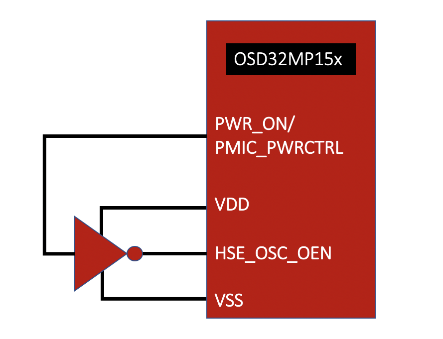
| RC2 | ✓ | Enable HSE: Add a test point or DNP pull-down resistor footprint on HSE_OSC_OEN pin(1). For low power modes, connect PWR_ON/PMIC_PWRCTRL to HSE_OSC_OEN through an external inverter as shown in the HSE Low Power Connection Example. | |
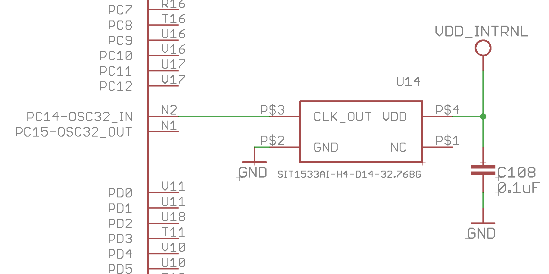
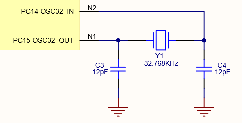
| RC3 | ✓ | LSE (OSC32) Connections: Use one of the example circuits shown in the OD32MP1-RED example or in the OSD32MP1-BRK example. | |
| RC4 | ✓ | LSE (OSC32) Unconnected: If no external crystal or oscillator is connected, leave pins PC14-OSC32_IN and PC15-OSC32_OUT floating |
Boot Configuration
| Topic No. | OSD32MP15x | SCHEMATIC CHECKLIST TOPIC – Mandatory | |
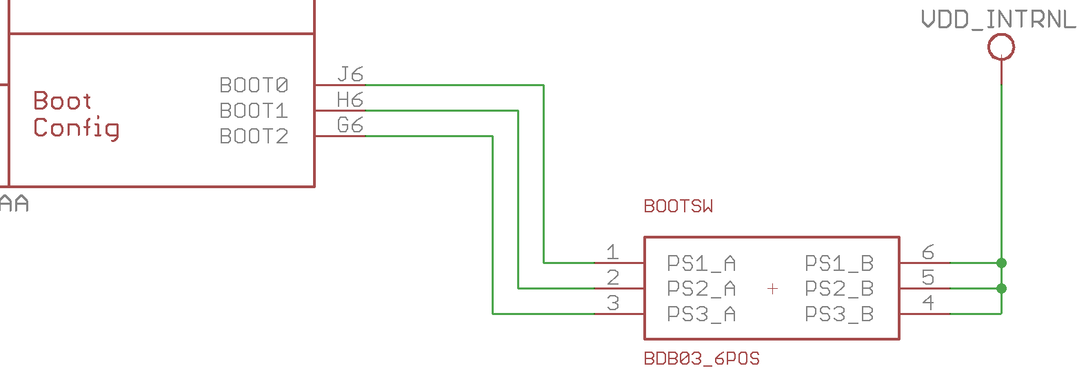
| BC1 | ✓ | Boot Mode: Make provisions to set appropriate Boot Modes as needed as shown in the Boot Configuration Example. See commonly used Boot Modes in the Boot Modes table. For a more detailed list (UART, NAND, NOR boot etc), see Table 2 of STM32MP15x datasheet. Default pins used by ROM code for each boot mode can be found in STM32MP15 ROM code overview app note. |
| Topic No. | OSD32MP15x | SCHEMATIC CHECKLIST TOPIC – Recommended | |
| BC2 | ✓ | Resistors: Weak internal pull-down resistors are enabled for all BOOT pins by default (1). Externally pull up only those pins that need to be set “1” or “HIGH”. See the Boot Configuration Example. |
USB
| Topic No. | OSD32MP15x | SCHEMATIC CHECKLIST TOPIC – Mandatory | |
| UB1 | ✓ | USB Routing: USB_DPx and USB_DMx traces must be length matched between the OSD32MP15x and the USB endpoint or connector with minimal stubs. See section 10.1.12 of Getting Started with STM32MP1 Hardware Development app note for potential use cases (1) (2) | |
| UB2 | ✓ | USB Termination Resistors: There should be no series resistors on USB_DPx and USB_DMx lines. Additionally, do not add any external capacitors to the USB lines. | |
| UB3 | ✓ | USB Host Mode Power: Use PMIC_BSTOUT or PMIC_VBUSOTG output rails to power external USB devices in Host Mode. See the Power Input table for more info on how to use/enable these power switches. See Figure 48, 50, 51 and 52 of STPMIC1 datasheet (2) | |
| UB4 | ✓ | USB ID Connection: Use pinPA10 as the OTG_HS_ID/OTG_FS_ID pin USBx_ID pin values: Host Mode Pulled to Ground Client Mode Floating OTG Mode Connected to USB client connectorNote: The OSD32MP1-BRK does not follow this recommendation. Please follow what has been outlined here. | |
| UB5 | ✓ | USB VBUS detection: Connect OTG_VBUS pin to VBUS rail of client/peripheral/OTG USB port. This analog input pin will detect the presence of a valid Host on the client/peripheral/OTG USB port. See section 10.1.12 of STM32MP15x Hardware Getting Started Guide. | |
| UB6 | ✓ | USB1 Host Only: The USB1 Port of the can only be configured as an USB Host Port. Please refer to https://wiki.st.com/stm32mpu/wiki/USBPHYC_internal_peripheral for more information. |
(2) Make sure the current sink from PMIC_BSTOUT, PMIC_VBUSOTG and PMIC_SWOUT rails of OSD32MP15x SiP does not exceed maximum ratings mentioned in Table 8-2 of OSD32MP15x datasheet.
eMMC
| Topic No. | OSD32MP15x | SCHEMATIC CHECKLIST TOPIC – Mandatory | |
| MC1 | ✓ | eMMC Pull-up Resistors: Use 10K – 50K pull-up resistors on RST#, CMD, and all DAT signals |
| Topic No. | OSD32MP15x | SCHEMATIC CHECKLIST TOPIC – Recommended | |
| MC2 | ✓ | eMMC Termination Resistors: Include a 22ohm series resistor on MMCx_CLK signals close to the processor to eliminate possible reflections and false clock transitions | |
| MC3 | ✓ | eMMC Connections: The STM32MP15x supports the MMC v4.51 interface so only those signals must be connected. Any MMC v5.x signals do not need to be connected. | |
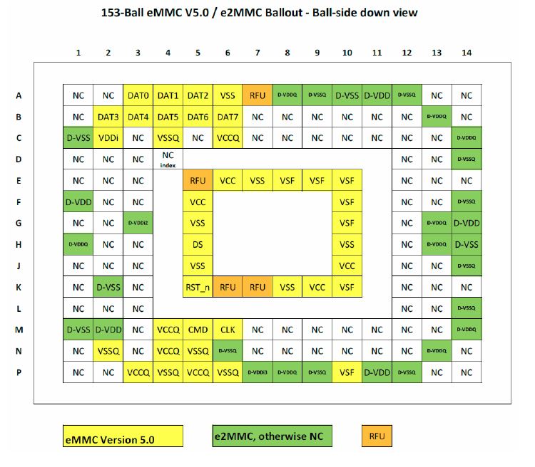
| MC4 | ✓ | eMMC Routing: In the eMMC Pinout, the “No Connect” (NC) pins can be routed through but “Reserved for Future Use” (RFU) pins should not be routed through to allow larger trace widths when routing the eMMC | |
| MC5 | ✓ | App Notes: Check if any app notes listed under section 3.3.3 applies to your design |
Other interfaces
| Topic No. | OSD32MP15x | SCHEMATIC CHECKLIST TOPIC – Mandatory | |
| IO1 | ✓ | Pin Mapping: If porting from STM32MP15x design, verify the pin mapping between STM32MP15x and OSD32MP15x using OSD32MP15x Family Pin Assignments app note | |
| IO2 | ✓ | Pin Muxing: Verify pin mux settings and avoid pin conflicts using CubeMX Pin Map GUI. | |
| IO3 | ✓ | UART Requirements: Implement Null Modem for all UART devices (i.e. TX -> RX; RX -> TX; CTS -> RTS; RTS -> CTS; DTR -> DSR; DSR -> DTR) | |
| IO4 | ✓ | SPI Requirements: Each SPI device should have its own Chip Select (CS) | |
| IO5 | ✓ | I2C Requirements: All I2C busses must be pulled up (1) | |
| IO6 | ✓ | JTAG Requirements: Refer OSD32MP1-BRK or OSD32MP1-RED schematic for recommended JTAG connections (2). | |
| IO7 | ✓ | EEPROM Write Protect: Connect EEPROM_WP pin to either an external test point or ground jumper or external control logic. EEPROM_WP needs to be pulled low in order to write to the EEPROM |
(2) TC2050-IDC-NL 10-pin cable and TC2050-ARM2010 adapter required to use Tag Connect JTAG interface with ST-Link/v2 or ST-Link v3 external debugger/programmer.
| Topic No. | OSD32MP15x | SCHEMATIC CHECKLIST TOPIC – Recommended | |
| IO8 | ✓ | Unused IO: Leave unused I/O and unused peripheral pins floating | |
| IO10 | ✓ | MII Termination Resistors: Add termination resistor footprints for TX and RX lines of MII/RMII/RGMII interfaces. | |
| IO14 | ✓ | App Notes: Check if any app notes listed under section 3.3.4 applies to your design |
Appendix
Use Cases
Power Input
| Use Case | Power Inputs | Source Connection | Sink Connection | |||
| VIN | PMIC_ LDO25IN | PMIC_ BSTIN | PMIC_ SWIN | |||
| 1 | ✓ | ✗ | ✗ | ✗ | Connect VIN Connect PMIC_LDO25IN Connect PMIC_BSTIN (5) Connect PMIC_SWIN | to DC Power Supply (4) to nothing (i.e. leave floating) to nothing (i.e. leave floating) to nothing (i.e. leave floating) |
| 2 | ✓ | ✗ | ✓ | ✗ | Connect VIN Connect PMIC_LDO25IN Connect PMIC_BSTIN (5) Connect PMIC_SWIN | to DC Power Supply (4) to nothing (i.e. leave floating) to VIN (2)(3) to nothing (i.e. leave floating) |
| 3 | ✓ | ✗ | ✓ | ✓ | Connect VIN Connect PMIC_LDO25IN Connect PMIC_BSTIN (5) Connect PMIC_SWIN | to DC Power Supply (4) to nothing (i.e. leave floating) to VIN (2)(3) to VIN (2)(3) |
| 4 | ✓ | ✓ | ✗ | ✗ | Connect VIN Connect PMIC_LDO25IN Connect PMIC_BSTIN (5) Connect PMIC_SWIN | to DC Power Supply (4) to VIN (1) to nothing (i.e. leave floating) to nothing (i.e. leave floating) |
| 5 | ✓ | ✓ | ✓ | ✗ | Connect VIN Connect PMIC_LDO25IN Connect PMIC_BSTIN (5) Connect PMIC_SWIN | To DC Power Supply (4) to VIN (1) to VIN (2)(3) to nothing (i.e. leave floating) |
| 6 | ✓ | ✓ | ✓ | ✓ | Connect VIN Connect PMIC_LDO25IN Connect PMIC_BSTIN (5) Connect PMIC_SWIN | To DC Power Supply (4) to VIN (1) to VIN (2)(3) to VIN (2)(3) |
(2) Boost converter is most useful to supply power to USB sub-system in battery powered designs. For example use cases, see section 4.6, figures 50, 51 and 52 of STPMIC1 datasheet.
(3) Boost converter, PWR_USB_SW and PWR_SW power switches are disabled by default on STPMIC1 power up. They can only be enabled by I2C setting of corresponding BST_ON, VBUSOTG_ON or SWOUT_ON bit in BST_SW_CR register of STPMIC1.
(4) STPMIC1A supports an input voltage range of 2.8V to 5V. However, the default input voltage threshold is 3.5V. To change this to allow lower input voltages, see the STPMIC1 NVM Programming app note.
(5) PMIC_VBUSOTG output rail can be used only when PMIC_BSTIN is powered since STPMIC1A’s PWR_USB_SW power switch is internally sourced by PMIC_BSTOUT.
VBAT
| Use Case | VBAT operation | Required connections |
| 1 | Not required | Connect VBAT pin to VDD |
| 2 | Required – using external battery/super cap (1.2V – 3.6V) | Connect VBAT pin directly to external battery/super cap |
| 3 | Required – using external battery/super cap (>3.6V) | Use an external LDO to bring down voltage of battery/super cap within acceptable range (1.2V-3.6V) and then feed it to VBAT pin |
Boot Modes
| BOOT2 | BOOT1 | BOOT0 | Initial Boot Mode* | Comments |
| 1 | 0 | 1 | SD-Card on SDMMC1 | SD boot |
| 0 | 1 | 0 | eMMC on SDMMC2 | eMMC boot |
| 0 | 0 | 0 | UART/USB | Can be used for flashing SD card using ST’s Cube Programmer |
| 1 | 0 | 0 | Debug/Engg Mode/Reserved | Can be used to directly program M4 core using JTAG + ST Linkv2/v3 debugger |
| 0 | 0 | 1 | Serial NOR Flash | Serial NOR Flash on QUADSPI |
| 0 | 1 | 1 | NAND Flash | SLC NAND Flash on FMC |
| 1 | 1 | 1 | Serial NAND Flash | Serial NAND Flash on QUADSPI |
Reference Figures
HSE Low Power Connection Example
LSE (OSC32) Circuit Examples
Boot Configuration Example
eMMC Pinout
For more details, please see our app note on Designing for Flexibility Around eMMC.
Useful Generic App Notes and Links
ST App Notes
- Getting Started with STM32MP1 Hardware Development: https://www.st.com/resource/en/application_note/dm00389996-getting-started-with-stm32mp151-stm32mp153-and-stm32mp157-line-hardware-development-stmicroelectronics.pdf
Power Design
- OSD32MP15x Power System Overview:
https://octavosystems.com/app_notes/osd32mp1-power-system-overview/ - OSD32MP15x Power Budgeting:
https://octavosystems.com/app_notes/osd32mp1-power-budgeting/ - OSD32MP15x Low Power Modes:
https://octavosystems.com/app_notes/osd32mp1-low-power-modes/ - STPMIC1 Non-Volatile Memory Programming Guide: https://octavosystems.com/app_notes/stpmic1-non-volatile-memory-programming-guide/
MMC
- OSD335x eMMC Application Note*: https://octavosystems.com/app_notes/designing-for-flexibility-around-emmc/
- OSD335x Design Tutorial Lesson 2*: Adding Non-Volatile Storage https://octavosystems.com/app_notes/osd335x-lesson-2-adding-non-volatile-storage/
GPIO and Other Interfaces
- OSD335x Peripheral Circuitry tutorial*: https://octavosystems.com/app_notes/osd335x-design-tutorial/bare-minimum-boot/peripheral-circuitry/
- Texas Instruments JTAG resource*: http://dev.ti.com/tirex/#/?link=Development%20Tools%2FDebug%20Probes%2FXDS%2FDocuments%2FJTAG%20Connectors
References
- OSD32MP15x Datasheet: https://octavosystems.com/docs/osd32mp15x-datasheet/
- OSD32MP15x Power Application Note: https://octavosystems.com/app_notes/osd32mp1-power-budgeting/
- STM32MP157 Datasheet: https://www.st.com/resource/en/datasheet/stm32mp157c.pdf
- STM32MP157 Reference Manual: https://www.st.com/resource/en/reference_manual/dm00327659-stm32mp157-advanced-armbased-32bit-mpus-stmicroelectronics.pdf
- STPMIC1 Datasheet: https://www.st.com/resource/en/datasheet/stpmic1.pdf
- ST Wiki: wiki.st.com
Contact Us
Please contact us on the forums for assistance with any checklist items or to tell us more things you’d like to see on this list. Our team is ready with more than a good-luck charm to help you with your designs. https://octavosystems.com/forums/
Revision History
Get notified of updates to this Application Note and all of our Technical Documentation.
"*" indicates required fields
| Revision Number | Revision Date | Changes | Author |
| 1 | 08/17/2020 | Initial Release | Eshtaartha Basu |
| 2 | 01/28/2021 | Multiple Additions for Clarity. | Greg Sheridan |
