OSD32MP1 Power System Overview
Published On: September, 9, 2020 By: Neeraj Dantu
The OSD32MP15x, the STM32MP15x System in Package (SiP), contains the STPMIC1A Power Management Integrated Circuit (PMIC) for power management. The PMIC is responsible for powering the STM32MP15x processor, Oscillator, EEPROM, and DDR. It provides configurable power-up and power-down sequencing required by the processor through programmable non-volatile memory (NVM). The PMIC contains six (6) adjustable LDOs, four (4) adjustable Buck convertors and one (1) Boost converter. The OSD32MP15x integrates the PMIC as well as the interface between the STM32MP15x and STPMIC1A for configuration.
This application note describes the hardware configuration of the OSD32MP15x and how the STPMIC1A and STM32MP15x are connected within the OSD32MP15x. It also describes the features and functions of the STPMIC1A inside of the SiP. It is designed to be an introduction to the power system of the OSD32Mp1 that can be used to optimize power consumption leveraging different low power modes and when creating a power budget.
Table of Contents
OSD32MP15x PMIC Hardware
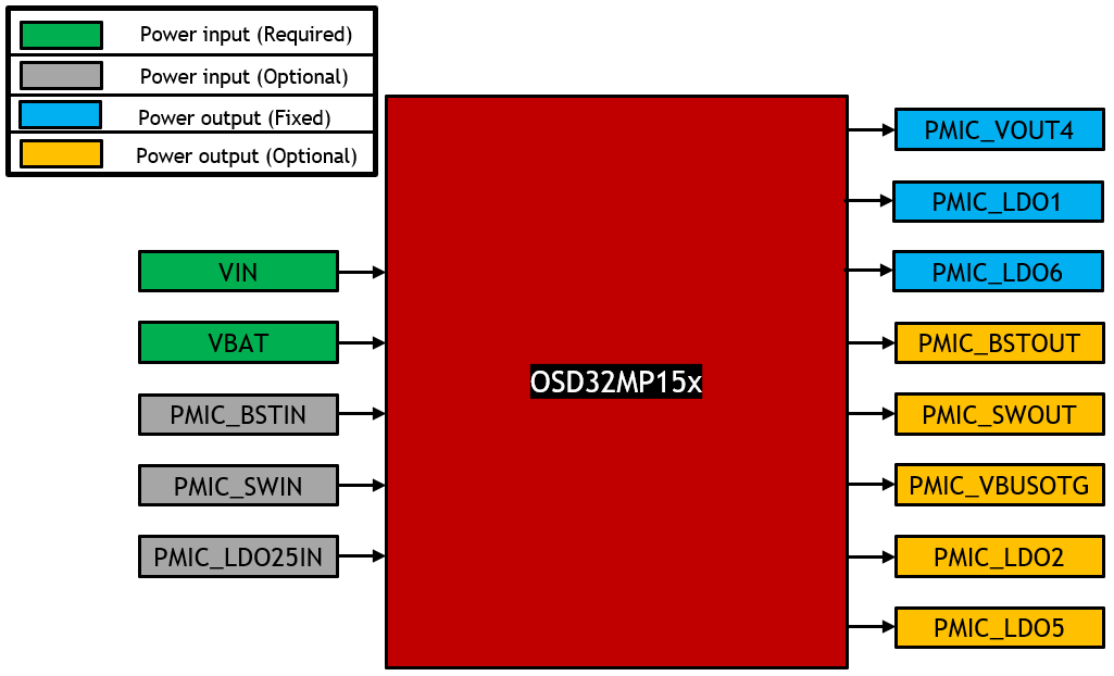
The OSD32MP15x has two required power inputs: VIN, the main power input, and VBAT, the backup battery power input. There are additional optional power inputs for system power outputs. The figure below shows the power inputs and output of the OSD32MP15x.
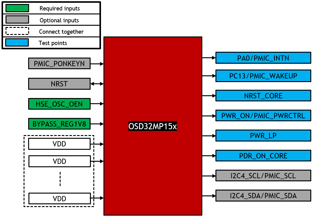
The OSD32MP15x integrates the connections between STM32MP15x and STPMIC1A to minimize the external connections required in the design. The figure below shows the OSD32MP15x pins for the power subsystem. Specifically, it shows pins that require external configuration, pins that can be optionally configured, and pins that have been internally connected and brought out as test points. Note that all the VDD pins of OSD32MP15x need to be tied together for the device to function properly. The Power Configuration Pins table describes the intended function of each of these pins and their role in OSD32MP15x.
| PIN | STM32MP15x FUNCTION | OSD32MP15x FUNCTION |
|---|---|---|
| PMIC_PONKEYN | Active Low user Power ON Key | Internally pulled up |
| NRST | Bidirectional pad reset allowing reset of external devices or reset of the device | Same as STM32MP15x. Connected to STPMIC1A RSTN |
| HSE_OSC_OEN | Active Low HSE oscillator enable (24MHz) | Pull to GND to enable internal oscillator |
| BYPASS_REG1V8 | Enable/Disable internal 1.8V regulator | External pull-down to GND required |
| PA0/PMIC_INTN | PA0 configured as WKUP1 – Used to wake-up from low power modes | Test point. Connected to STPMIC1A INTN |
| PC13/
PMIC_WAKEUP |
PC13 configured as RTCOUT1 – wake-up during VBAT mode | Test point. Connected to STPMIC1A WAKEUP |
| NRST_CORE | VDD_CORE reset input (to be used when VDD_CORE Power on Reset is disabled) | Test point. Has a 10nF capacitor |
| PWR_ON/
PMIC_PWRCTRL |
PWR_ON – Low power control signal | Test point. Connected to STPMIC1A PWRCTRL |
| PWR_LP | VDD_CORE low power control | Test point. Unused |
| PDR_ON_CORE | VDD_CORE power on reset enable | Test point. Pulled up to VDD |
| I2C4_SCL/
PMIC_SCL |
PMIC I2C control interface clock | Can be used to connect to other I2C devices.
Test point if not used externally. |
| I2C4_SDA/
PMIC_SDA |
PMIC I2C control interface data |
The figure below shows the internal power system of the OSD32MP15x with all the power connections between the PMIC and the power domains of the processor. This internal configuration makes it possible for OSD32MP15x to have a simple external power configuration circuit described in the Power Inputs and Outputs and the Pin Configuration figures.
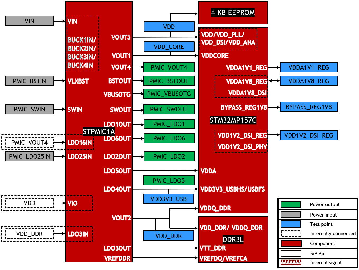
As can be seen from the above figures, the OSD32MP15x provides several output power rails. Some of them power the internal subsystems of the SiP and are purely test points on the boundary of the SiP and some of them are available for devices on board external to the SiP. The table below shows the voltage output levels of each of the voltage sources. All VOUTx and LDOx output voltages can be changed dynamically using I2C commands when the PMIC is in active mode. If you wish to change these voltages, you must reprogram the BUCKS_VOUT_SHR (VOUTx) and LDOS_VOUT_SHRx (LDOx) registers in the PMIC non-volatile memory (NVM). The process is detailed in the PMIC Reprogramming Application Note and ST’s PMIC programming guide.
| STPMIC1 | OSD32MP15x Voltage rail | Default output voltage(V) | OSD32MP15x output Voltage (V) | Ranks |
|---|---|---|---|---|
| VOUT1 | VDDCORE | 1.2 | 1.2 | 2 |
| VOUT2 | VDD_DDR | 1.1 | 1.35 | 0 |
| VOUT3 | VDD | 3.3 | 1.8/3.3 | 1 |
| VOUT4 | PMIC_VOUT4 | 3.3 | 0.6 – 3.9 or VIN | 2 |
| LDO1OUT | PMIC_LDO1 | 1.8 | 1.7 – 3.3 or PMIC_VOUT4 | 0 |
| LDO2OUT | PMIC_LDO2 | 1.8 | 1.7 – 3.3 | 0 |
| LDO3OUT | VTT_DDR | 1.8 | 0.675 | 0 |
| LDO4OUT | VDD3V3_USBHS | 3.3 | 3.3 | 3 |
| LDO5OUT | VDDA | 2.9 | 1.7 – 3.9 | 2 |
| LDO6OUT | PMIC_LDO6 | 1.0s | 0.9 – 3.3 or PMIC_VOUT4 | 0 |
| BSTOUT | PMIC_BSTOUT | 5.2 | 5.2 | N/A |
| VBUSOTG | PMIC_VBUSOTG | 5.2 | 5.2 | N/A |
| SWOUT | PMIC_SWOUT | SWIN | PMIC_SWIN | N/A |
| VREFDDR | VREFDQ | 0.55 | 0.675 | 0 |

The following legend shows the configuration options of each of the output power rails according to the color coding of their row in the Power Output Configuration table:
| Internal outputs. Fixed voltage. Must be enabled. Test point only. |
| Configurable voltage but limited to either 1.8V or 3.3V. Can be used for external configuration (pull-up/pull-down). Must be enabled. |
| User outputs. Configurable voltage. |
| User outputs. Fixed voltage. |
PMIC Features and Functions
Power up/Power Down Sequence
The default power-up/power down sequence of the PMIC is shown in the table below.
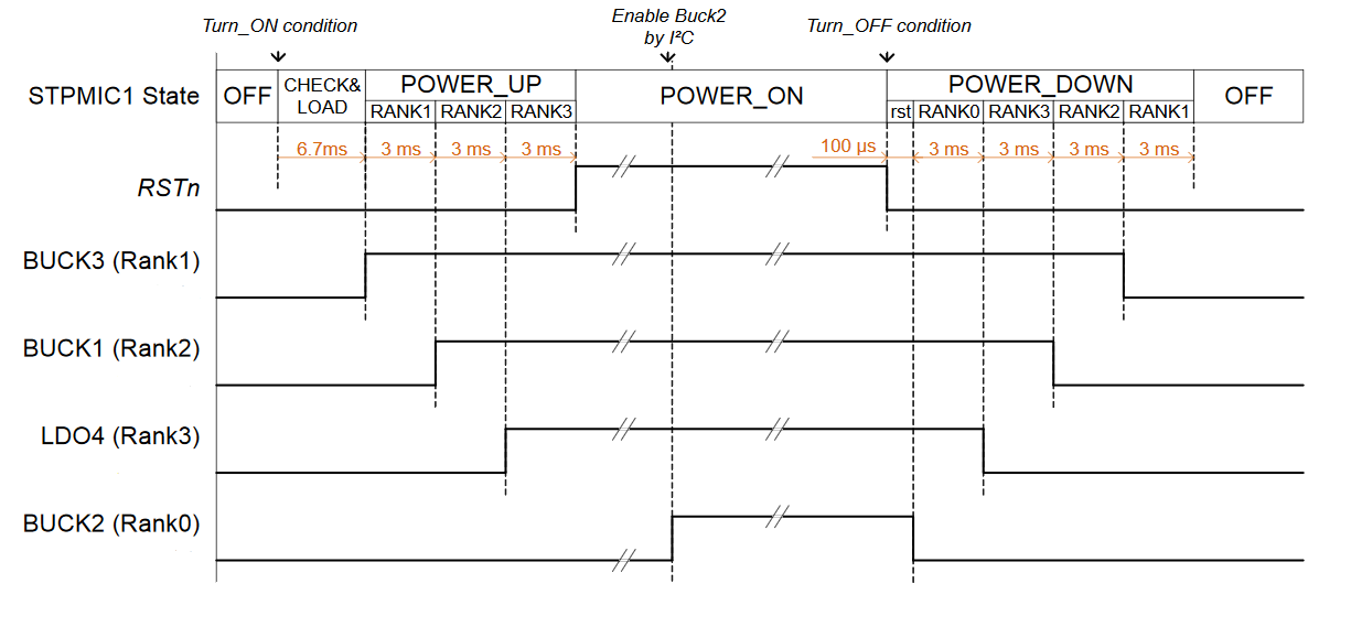
The order in which output power rails are activated is determined by Rank. Automatically, Rank1 powers up first, Rank2 powers up second, and Rank3 powers up last. However, Power rails with Rank0 do not power up automatically, and must be enabled after the device has booted using the PMIC I2C interface.
Turn-ON Conditions
The Turn-ON condition in the Power-up/Power-down Sequence figure refers to one of the following:
- PONKEYn pin detection (falling edge)
- VBUS detection (voltage on VBUSOTG or SWOUT above VBUSOTG_Rise or SWOUT_Rise, respectively. These conditions can be disabled.)
- WAKEUP pin detection (rising edge)
The Auto turn-ON feature of the STPMIC1A allows it to transition to the POWER_ON state if VIN rises above VINOK_Rise. See the VIN Threshold table and the STPMIC1A State Machine diagram for more information.
Turn-OFF Conditions
The Turn-OFF condition in the Power-up/Power-down Sequence figure refers to one of the following:
- Software switch OFF with SWOFF bit in MAIN_CR register of the PMIC
- PONKEYn long press
- Thermal shutdown
- Overcurrent protection
- Watchdog timer expiration
- VIN falls below VIN_OK_Fall (See the VIN Threshold table for more information)
The Turn-OFF feature of the STPMIC1A allows it to transition to the OFF state. See the STPMIC1A State Machine diagram for more information.
VIN Thresholds
To trigger certain PMIC events, like Turn-ON and Turn-OFF conditions, the voltage of the VIN power input must rise above or fall below certain voltage thresholds. The following figure shows the different threshold triggers of STPMIC1A:
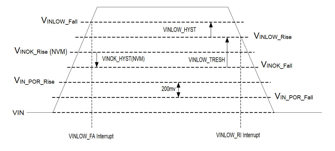
The four thresholds that most affect customer applications are: VIN_POR_Rise, VIN_POR_Fall, VINOK_Rise and VINOK_Fall. The table below provides the definitions and specifications for these thresholds for the OSD32MP15x device which uses the STPMIC1A.
| NAME | DESCRIPTION | PMIC REGISTER | THRESH |
| VIN_POR_Rise | VIN > VIN_POR_Rise means
PMIC is in a functional state |
Not modifiable | 2.3V |
| VIN_POR_Fall | VIN < VIN_POR_Fall means
PMIC in NO_SUPPLY state |
Not modifiable | 2.1V |
| VINOK_Rise | VIN > VINOK_Rise means
PMIC in POWER_ON state |
NVM_MAIN_CTRL_SHR
to change threshold |
3.5V |
| VINOK_Fall | VIN < VINOK_Fall means
PMIC in POWER_OFF state |
NVM_MAIN_CTRL_SHR
to change threshold |
3.0V |
For more details on the different power states, see the STPMIC1A State Machine diagram.
Efficiencies of Power Rails
The table below shows the minimum efficiencies of the BUCK and BOOST converters of STPMC1A inside the OSD32MP15x. These efficiencies can be helpful in accurately determining the total power consumption of the board during power budgeting. Note that the efficiency listed is the minimum efficiency of the power rail. This efficiency is used to calculate a worst-case power scenario for all the converters.
| STPMC1A VOLTAGE RAIL | OSD32MP15x VOLTAGE RAIL | MINIMUM EFFICIENCY (%) |
|---|---|---|
| VOUT1 | VDD_CORE | 70 |
| VOUT2 | VDD_DDR | 84 |
| VOUT3 | VDD | 88 |
| VOUT4 | PMIC_VOUT4 | 79 |
| BSTOUT | PMIC_BSTOUT | 89 |
LDO Dropout Voltages
The table below shows the maximum dropout voltages for each of the four programmable LDOs of OSD32MP15x. These dropout voltages must be considered when setting the output voltages of these LDOs in the kernel device tree. For LDO2 and LDO5, the input voltage is provided externally through PMIC_LDO25IN. For LDO1 and LDO6, the input voltage is provided by PMIC_VOUT4. Therefore, the output voltage of each LDO must be less than the input voltage minus the dropout voltage. For example, if PMIC_VOUT4 is configured to be 3.3V, then the maximum voltage of LDO1 and LDO6 is 3.0V.
| STPMC1A VOLTAGE RAIL | OSD32MP15x VOLTAGE RAIL | MAXIMUM DROPOUT VOLTAGE (mV) |
|---|---|---|
| LDO1OUT | PMIC_LDO1 | 300 |
| LDO2OUT | PMIC_LDO2 | 300 |
| LDO5OUT | VDDA | 300 |
| LDO6OUT | PMIC_LDO6 | 300 |
STPMIC1A State Machine
The PMIC has a fixed start up and power down sequence described by a state machine. The figure below shows the state machine diagram for STPMIC1A.
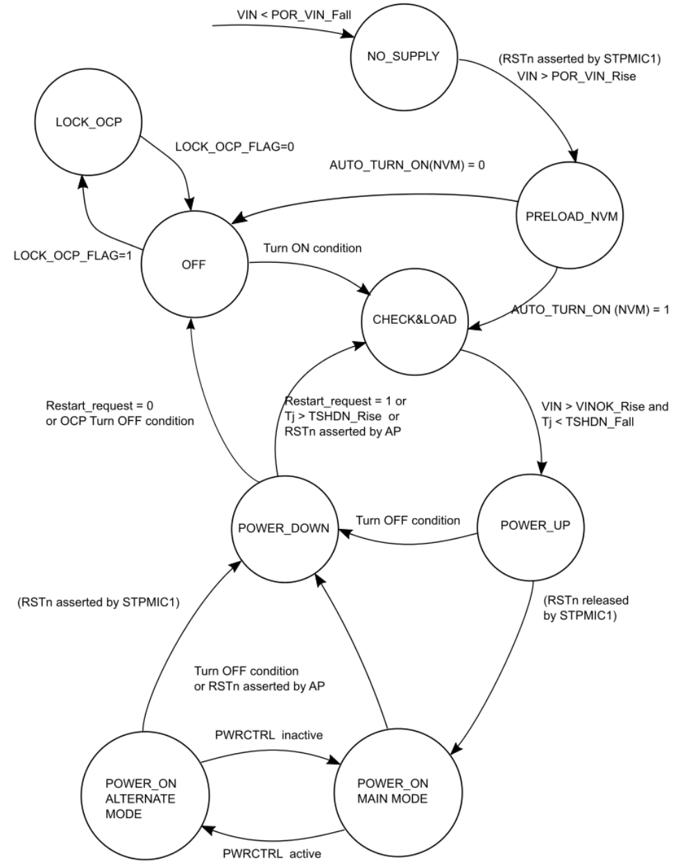
To better understand each state, a description is provided in the following table.
| STATE | DESCRIPTION |
|---|---|
| NO_SUPPLY | STPMIC1A is not functional |
| PRELOAD_NVM | Non-Volatile memory (NVM) read operation is performed to check for AUTO_TURN_ON bit |
| OFF | STPMIC1A regulators are OFF |
| LOCK_OCP | Power down mode after overcurrent has been detected on STPMIC1A power rails |
| CHECK&LOAD | Thermal monitoring is started. STPMIC1A registers are loaded from internal Non-Volatile Memory (NVM). VIN monitoring is started. RSTn is asserted and all STPMIC1A regulators are OFF |
| POWER_UP | STPMIC1A started output regulators. RSTn is asserted |
| POWER_ON | There are two modes: MAIN_MODE and ALTERNATE_MODE depending on the PWRCTRL input (connected to PWR_ON output of STM32MP1). RSTn is released and monitored |
| POWER_DOWN | All STPMIC1A output power rails are turned OFF |
Some important points to be aware of for the OSD32MP15x:
- By default, VINOK_Rise threshold is set to 3.5V. It can be changed by modifying the NVM of the PMIC. See the VIN Thresholds section for more information.
- By default, the AUTO_TURN_ON bit in the NVM of STPMIC1A is set to 1. So, the PMIC proceeds to the CHECK&LOAD state immediately after PRELOAD_NVM.
- Turn-ON conditions are listed in Turn-ON Conditions section.
- Turn-OFF conditions are listed in Turn-OFF Conditions sections.
For more information, see Section 5.2 of STPMIC1A Datasheet.
Conclusion
This document discussed the power management system of OSD32MP15x and its many features. If you have other questions, please visit our forums.
Revision History
Get notified of updates to this Application Note and all of our Technical Documentation.
"*" indicates required fields
| Revision Number | Revision Date | Changes | Author |
| 1 | 09/02/2020 | Initial Release | Justin Berry, Neeraj Dantu |