OSDZU3 Schematic Checklist
Published On: September, 19, 2023 By: Eshtaartha Basu | Updated: October 25, 2023 by Greg Sheridan
The OSDZU3 System-In-Package (SiP) product consists of building blocks designed to allow easy and cost-effective implementation of systems based on AMD’s XCZU3 Ultrascale+™ MPSoC. The OSDZU3 integrates the XCZU3 MPSoC along with two Infineon PMICs, two LDOs, up to 2 Gigabyte (GB) of LPDDR4 Memory, a QSPI Flash Memory, an EEPROM for non-volatile configuration storage, resistors, capacitors, and inductors into a single 20.5mm x 40mm design-in-ready package.
This document provides a checklist to help designers review the schematics built around the OSDZU3. Going through this checklist before or during the schematic design phase will help avoid common pitfalls. This OSDZU3 schematic checklist assumes a generic embedded system knowledge and is therefore not exhaustive. Each design is unique, and a custom design may require additional in-depth verification to validate its overall functionality.
This document consists of multiple checklists to help validate each sub-section of a design. To get started, here is a list of the top-level checklists:
| ITEM | SCHEMATIC CHECKLIST TOPIC | |
|---|---|---|
| ✓ | 1 | Essential Connections and Power Design |
| ✓ | 2 | SYSMON Power Configuration |
| ✓ | 3 | Clock Signals |
| ✓ | 4 | Boot Configuration |
| ✓ | 5 | Non-Volatile Memory Configuration |
| ✓ | 6 | IO Interfaces |
Notice: The information provided within this document is for informational use only. Octavo Systems provides no guarantees or warranty to the information contained.
The Appendix of this document lists useful reference documents along with tables and figures that may be of use to you as you use this check list.
Finally remember to take advantage of the OSDZU3 layout guide as you begin to realize your schematic into a PCB layout.
Table of Contents
OSDZU3 Schematic Checklist
Essential Connections and Power Design
The OSDZU3 SiP is designed to give flexibility on how to power it. Inside the SiP there are two Power Management Integrated Circuits (PMICs) and two Low Drop Out (LDO) linear regulators. The SiP requires a single primary 5-volt input supply. In addition to the primary 5-volt input supply there is an optional battery input for low power operation.
Some of the secondary input power rails of the OSDZU3 are brought out to the ball grid array to give you the flexibility to choose the power source and in some cases, the input voltage. These inputs must be preferably connected to a suitable OSDZU3 output power rail on the PCB. These power inputs are:
- Bank I/O Power Inputs
- SYSMON Power Inputs
| Topic No. | OSDZU3 | SCHEMATIC CHECKLIST TOPIC – Mandatory | |
|---|---|---|---|
| PD1 | ✓ | Input Power Connections: Choose a power input use case from the Power Input Table based on design requirements and implement mandatory connections | |
| PD2 | ✓ | In-Rush Current: The power source connected to the primary power input, +5V_IN, must be able to supply the necessary in-rush current: 1.5A. Note that OSDZU3 can consume current higher than inrush during operation based on use case. | |
| PD3 | ✓ | External Capacitors: See the ‘External Capacitors’ section of the OSDZU3 datasheet for the list of required external capacitors. See OSDZU3 Layout Guide for recommendations on capacitor placement. | |
| PD4 | ✓ | External Resistors: See the ‘External Resistors’ section of the OSDZU3 datasheet for the list of required external resistors. | |
| PD5 | ✓ | Bank I/O Voltage: The I/O power inputs for Banks 24 – 26, 44, 64 – 66 and 500 – 503 are not connected to internal power sources. They must be appropriately powered by either OSDZU3’s output power rails or external power sources. See the Topic No PD13 for power source recommendations. Also refer to the Bank Power Inputs section of the OSDZU3 Data Sheet. | |
| PD6 | ✓ | Bank 500 Power Input – VCCO_PSIO_500: VCCO_PSIO_500 must be connected to the same voltage as that of integrated QSPI IO. This is because the integrated QSPI is powered by VCCO_PSIO_500 power input and the QSPI uses Bank 500 IO. For detailed info on all the supported Bank 500/internal QSPI IO voltages and corresponding part numbers, see Option Designator sub section under Product Number Information section of OSDZU3 Datasheet. | |
| PD7 | ✓ | Bank 503 Power Input – VCC_PSIO_503: Bank 503 contains important configuration and status pins. So, VCCO_PSIO_503 must be connected to a valid voltage source. | |
| PD8 | ✓ | Bank VREF_x inputs:
| |
| PD9 | ✓ | Output Power Rails: Four output power rails are available for external usage – PMIC_1B, PMIC_2C, VCCAUX, VCC_PSAUX. Two rails (PMIC_1B, PMIC_2C) are user programmable. See ‘PMIC voltage output requirements for OSDZU3’ table and ‘Power Output’ section of OSDZU3 Datasheet for more info. Also see PMIC Programming Guide. | |
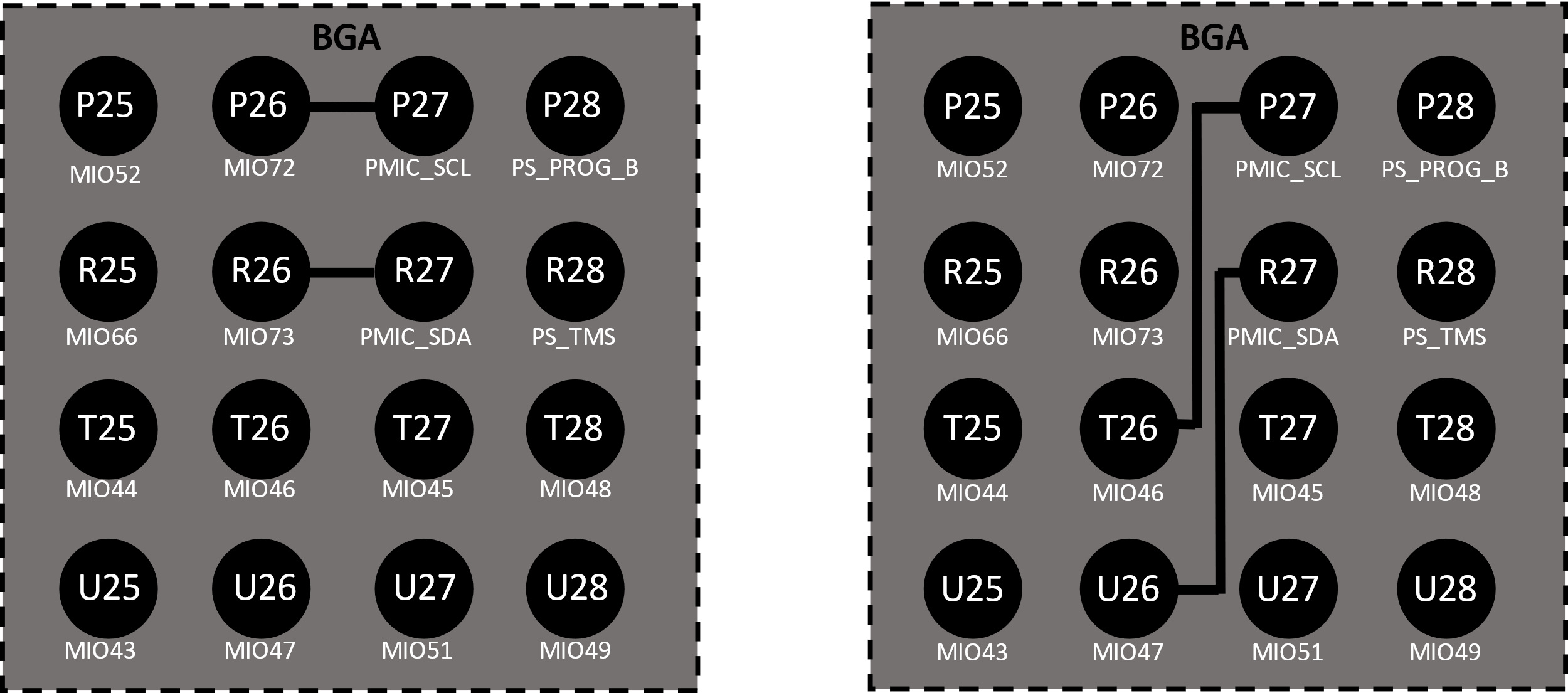
| PD10 | ✓ | XCZU3 Processor – PMIC Connections: To enable I2C communication between OSDZU3’s PMICs and ZU3, external connections between PMIC I2C bus i.e., PMIC_SCL, PMIC_SDA and ZU3’s I2C bus (example: MIO72 and MIO73 respectively or MIO46 and MIO47) MUST be made. See PMIC I2C Connection examples reference figure. Also see ‘PMIC Control and Communication Signals’ section and PMIC I2C Interconnect section of OSDZU3 Datasheet for more detailed info. | |
| PD11 | ✓ | VDDIO: VDDIO is the PMIC IO voltage. Connect this input to a valid 3.3V source (for example +3V3_ON). | |
| PD12 | ✓ | VCC_PSBATT Operation: Choose one of the use cases from the Power Input Table. | |
| PD13 | ✓ | VCC_PSDDR_PLL: VCC_PSDDR_PLL is a 1.8V nominal supply that provides power to the PLL used for the PS DDR Controller. It must be connected to a noise filtered 1.8V source (for example VCC_PSAUX). | |
| PD14 | ✓ | PMIC MTP (NVM Select) connections: External resistors to GND are required on PMIC1_MTP and PMIC2_MTP pins. See ‘ZU3 Ball Descriptions for Miscellaneous Signals’ table of OSDZU3 Datasheet for recommended resistor values. Also see PMICx_MTP section of OSDZU3 PMIC Programming Guide |
| Topic No. | OSDZU3 | SCHEMATIC CHECKLIST TOPIC – Recommended | |
|---|---|---|---|
| PD15 | ✓ | Choosing IO Bank Input Power Source:
| |
| PD16 | ✓ | Bank I/O Power Input External Capacitors: (47µF + 10 µF) external capacitance per bank power input of HDIO/HPIO is recommended. When using same IO voltage, one 47µF capacitance can be shared per every 4 HPIO/HDIO banks. (100µF + 10 µF) external capacitance per bank power input of PSIO is recommended. When using same IO voltage, one 100µF capacitance can be shared per every 4 PSIO banks. | |
| PD17 | ✓ | PMIC_IRQB connection: Add a test point or route this pin to one of the GPIOs of OSDZU3 or an external supervisor to get alerts of PMIC faults. Please note that this pin is Open Drain output of the PMICs that is pulled up to VDDIO inside the SiP. | |
| PD18 | ✓ | PWR_EN connection: Add a test point or jumper to this pin (to connect it to GND) to allow for easy PMIC re-programming in prototype phase or disabling all PMIC outputs when needed. Note that this PMIC input pin is pulled up to +3V3_ON inside the SiP. | |
| PD19 | ✓ | PGOOD Connection: Add test point or LED for debug purposes to indicate when 1 of the PMICs experiences power rail failure. This pin is connected to PS_POR_B and pulled up to VCCO_PSIO_503 inside the SiP. | |
| PD20 | ✓ | Power Budget: Create a Power Budget for your design using the OSDZU3 Power Application Note | |
| PD21 | ✓ | Test Points: Make sure the following signals are accessible for debugging. If they are not, add a test point on each of the following signals if possible: PMIC Signals: PMIC_IRQB, PWR_EN, PGOOD, PMIC_SLEEP, VDDIO Clock Signals: OSC_OE, PS_PADI, PS_PADO, PS_REF_CLK Power Rails: PMIC2_C, PMC1_B, VCCAUX, VCC_PSAUX, VCCINT, VCC_PSINTLP, VCC_PSINTFP, +3V3_ON, VCC_ADC, VCC_PSADC, VCC_PSPLL, VCCO_PSDDR, +MGTRAVCC, +MGTRAVTT, VCCO_PSIO_X, VCCO_HDIO_X, VCCO_HPIO_X, VREFP Other Signals: EEPROM_WP, PUDC_B, POR_OVERRIDE, PS_MODE [0:3], PS_SRST_B, PS_POR_B, PS_PROG_B, PS_INIT_B, PS_DONE, PS_ERR_STAT, PS_ERR_OUT | |
| PD22 | ✓ | App Notes: Check if recommendations by app notes listed in the Useful Application Note Section applies to your design. |
SYSMON Power Configuration
| Topic No. | OSDZU3 | SCHEMATIC CHECKLIST TOPIC – Mandatory | |
|---|---|---|---|
| SM1 | ✓ | VCCADC input(1): Connect VCCADC to VCCAUX through ferrite bead to reduce noise. Additionally, we recommend placing 0.1µF capacitor, 470nF capacitor between VDDADC and GNDADC. See OSDZU3-REF design for good reference. | |
| SM2 | ✓ | GNDADC input(1): Connect GNDADC to GND through a ferrite bead to reduce noise on the ground connection. See OSDZU3-REF design for good reference. | |
| SM3 | ✓ | VCC_PSADC input(1): Connect VCC_PSADC to VCC_PSAUX through ferrite bead to reduce noise. Additionally, we recommend placing 0.1µF capacitor, 470nF capacitor between VCC_PSADC and GND_PSADC. See OSDZU3-REF design for good reference. | |
| SM4 | ✓ | GND_PSADC input(1): Connect GND_PSADC to GND through a ferrite bead to reduce noise on the ground connection. See OSDZU3-REF design for good reference. | |
| SM5 | ✓ | VREFP input: When VREFP is supplied by an external reference voltage, a 0.1µF capacitor must be added between VREFP and VREFN. See OSDZU3-REF design for good reference. | |
| SM6 | ✓ | GND_ANA connection: PMIC Analog Ground i.e., GND_ANA pins must be connected to VSS (GND) pins. |
(1) This connection is necessary even if SYSMON is unused.
Clock Signals
| Topic No. | OSDZU3 | SCHEMATIC CHECKLIST TOPIC – Mandatory | |
|---|---|---|---|
| C1 | ✓ | RTC External Resistor: To use the OSDZU3’s RTC, a 10Mohm resistor MUST be added externally between pins PS_PADI and PS_PADO. | |
| C2 | ✓ | Reference Clock Generator: Make provisions to externally supply 1.8V differential reference clocks for GTR interfaces you may be using depending on your use case to GTR_CLK_NX/ GTR_CLK_NX. See PS GTR & PL Ref Clock section of OSDZU3-REF design for recommendations on external reference clock generators. See Tables ‘Interconnect Matrix’ and ‘Reference Clock per Protocol’ in chapter ‘PS-GTR Transceivers’ of the MPSOC Reference Manual(UG1085). | |
| C3 | ✓ | OSC_OE: Add a test point on this pin for easy status validation of 33.33MHz internal oscillator and also have the flexibility to disable it, if necessary, in the prototype phase. Test point may not be necessary for production systems. |
Boot Configuration
| Topic No. | OSDZU3 | SCHEMATIC CHECKLIST TOPIC – Mandatory |
|---|---|---|
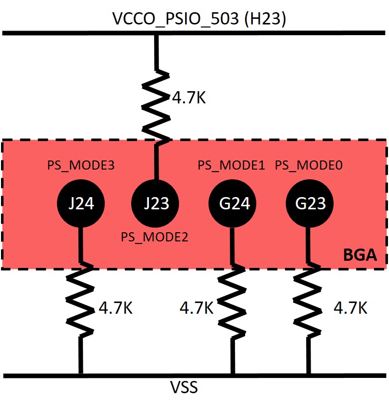
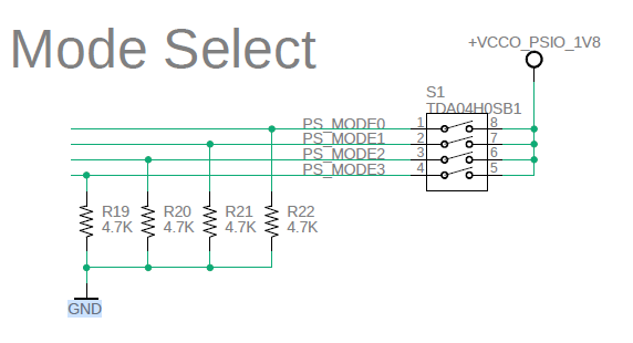
| BC1 | ✓ | Boot Mode Selection: Make provisions to set appropriate Boot Modes as needed as shown in the Boot Configuration Examples. See commonly used Boot Modes in the Boot Modes table. Also see ‘Mode selection’ section of the OSDZU3 datasheet for more info. |
Non-Volatile Memory
| Topic No. | OSDZU3 | SCHEMATIC CHECKLIST TOPIC – Mandatory | |
|---|---|---|---|
| NVM1 | ✓ | eMMC Boot @ 1.8V IO Only: eMMC boot is only supported when VCCO_PSIO_500 is connected to 1.8V and eMMC IOs are configured to operate at 1.8V. OSDZU3 will not be able to boot from the eMMC interface if VCCO_PSIO_500 is connected to a 3.3V rail. | |
| NVM2 | ✓ | Match Bank 500 and QSPI Voltage: OSDZU3’s internal QSPI is not dual voltage and will require either 3.3V or 1.8V. The OSDZU3 part number will specify the voltage level required by the QSPI. The voltage of VCCO_PSIO_500 MUST match the voltage required by the IO standard of the QSPI. | |
| NVM3 | ✓ | EEPROM I2C Connection: OSDZU3’s internal EEPROM is on the same I2C bus as the 2 PMICs (i.e., PMIC_SCL and PMIC_SDA). To use the EEPROM, PMIC_SCL and PMIC_SDA pins MUST be externally connected to ZU3’s I2C interface. See PMIC I2C Connection examples reference figure. Also see PMIC Control and Communication Signals section and PMIC I2C Interconnect section of OSDZU3 Datasheet for more detailed info. |
IO Interfaces
| Topic No. | OSDZU3 | SCHEMATIC CHECKLIST TOPIC – Recommended |
|---|---|---|
| IO1 | ✓ | PS-GTR Design check list: Schematic and PCB design checklist for MPSoC is provided by AMD here – https://docs.xilinx.com/r/en-US/ug583-ultrascale-pcb-design/PCB-Design-Checklist |
| IO2 | ✓ | PS_MGTRREF connection: Connect PS_MGTRREF to GND via a 500ohm, 0.5% resistor. |
| IO3 | ✓ | Pin Mapping: If porting from XCZU3 design, verify the pin mapping between XCZU3 and OSDZU3 using the OSDZU3 Data sheet. Also see OSDZU3 Ball Mapping to ZU3 app note. |
| IO4 | ✓ | Pin Muxing: Verify pin mux settings and avoid pin conflict. Refer to the AMD MIO Table at a Glance. Also refer to the OSDZU3 Data sheet. |
| IO5 | ✓ | UART Requirements: Implement Null Modem for all UART devices (i.e. TX -> RX; RX -> TX; CTS -> RTS; RTS -> CTS; DTR -> DSR; DSR -> DTR) |
| IO6 | ✓ | SPI Requirements: Each SPI device should have its own Chip Select (CS) |
| IO7 | ✓ | I2C Requirements: All I2C busses must be appropriately pulled up(1) |
| IO8 | ✓ | JTAG Requirements: Refer to OSDZU3-REF schematic for recommended JTAG connections. |
| IO9 | ✓ | EEPROM Write Protect: Connect EEPROM_WP pin to either an external test point or ground jumper or external control logic. EEPROM_WP needs to be pulled low in order to write to the EEPROM |
(1) PMIC I2C bus (PMIC_SCL and PMIC_SDA) has 10K internal pullups. Stronger external pullups are recommended if more than 2 external I2C devices are put on this bus.
| Topic No. | OSDZU3 | SCHEMATIC CHECKLIST TOPIC – Recommended |
|---|---|---|
| IO10 | ✓ | Unused IO: Leave unused IO peripheral pins floating |
| IO11 | ✓ | Bank 500 Config Pin Description: For a brief description of all the important Configuration pins in Bank 503 like JTAG, Boot Mode and Status pins, see ZU3 Ball Descriptions for Bank 503 section of OSDZU3 Datasheet. |
| IO12 | ✓ | Misc Pin Description: For a brief description of all the Miscellaneous pins like DXN, DXP, VN, VP etc., see ZU3 Ball Descriptions for Miscellaneous Signals section of OSDZU3 Datasheet. |
Appendix
Use Cases
Input power
The following table shows typical power input use cases.
| Use Case | Input | Source Connection | Sink Connection(1) | |||||
|---|---|---|---|---|---|---|---|---|
| +5V_IN | VSUPPLY | VDDIO | VCC_PSDDR_PL(2) | VCC_PSBATT | ||||
| 1 | P | P | P | P | O | Connect 5V (i.e., 4.5V – 5.5V) input power source | to +5V_IN | |
| to VSUPPLY | ||||||||
| Connect +3.3V_ON | to VDDIO | |||||||
| Connect +VCC_PSAUX_1V8 | to VCC_PSDDR_PLL(2) | |||||||
| Connect Nothing (i.e., floating) | to VCC_PSBATT | |||||||
| 2 | P | P | P | P | P | Connect 5V (i.e., 4.5V – 5.5V) input power source | to +5V_IN | |
| to VSUPPLY | ||||||||
| Connect +3.3V_ON | to VDDIO | |||||||
| Connect +VCC_PSAUX_1V8 | to VCC_PSDDR_PLL(2) | |||||||
| Connect “+” terminal of LR44 battery or +VCC_PSAUX_1V8 via diode. Note that valid voltage input for VCC_PSBATT is 1.2 – 1.5V | to VCC_PSBATT(3) | |||||||
(1) See External Capacitors section of OSDZU3 datasheet for recommended bulk capacitors.
(2) External ferrite bead and capacitor may be required for this input. See VCC_PSDDR_PLL section of OSDZU3 datasheet for more detailed info.
(3) Connect VCC_PSBATT to a LR44 battery or +VCC_PSAUX_1V8 via diode. See VCC_PSBATT circuitry of OSDZU3-REF schematics for good reference.
Boot Modes
| Boot Mode | Mode Pins (3:0) | Pin Location | CSU Mode | Description |
|---|---|---|---|---|
| PS JTAG | 0000 | JTAG | Slave | PSJTAG interface, PS dedicated pins. |
| Quad-SPI (24b) | 0001 | MIO (12:0) | Master | 24-bit addressing (QSPI24). |
| Quad-SPI (32b) | 0010 | MIO (12:0) | Master | 32-bit addressing (QSPI32). |
| SDO (2.0) | 0011 | MIO (25:21, 16:13) | Master | SD 2.0. |
| NAND | 0100 | MIO (25:09) | Master | Requires 8-bit data bus width. |
| SD1 (2.0) | 0101 | MIO (51:43) | Master | SD 2.0. |
| eMMC (1.8V) | 0110 | MIO (22:13) | Master | eMMC version 4.5 at 1.8V. |
| USB0 (2.0) | 0111 | MIO (52:63) | Slave | USB 2.0 only. |
| PJTAG (MIO #0) | 1000 | MIO (29:26) | Slave | PJTAG connection 0 option. |
| PJTAG (MIO #1) | 1001 | MIO (15:12) | Slave | PJTAG connection 1 option. |
| SD1 LS (3.0) | 1110 | MIO (51:39) | Master | SD 3.0 with a required SD 3.0 compliant voltage level shifter. |
Reference Figures
Boot Configuration Examples
The first figure shows Boot Mode configuration example with external pull-up and pull-down resistors only. The following figure shows the Boot Mode configuration from OSDZU3-REF design where pull-down resistors are used along with a four-pole switch to select the boot mode.
PMIC I2C Connection examples
The OSDZU3’s ball map is laid out to make the I2C connections between PMIC and ZU3 very easy as shown in the below figure. Either of the following configurations can be used.
Useful App Notes and Links
Octavo Systems Application Notes
- All application notes in one place – https://octavosystems.com/app_notes/#OSDZU3
- OSDZU3 Layout Guide – https://octavosystems.com/app_notes/osdzu3-layout-guide
- OSDZU3 Power application report – https://octavosystems.com/app_notes/osdzu3-power-application-note
- OSDZU3 Ball Mapping to ZU3 – https://octavosystems.com/app_notes/osdzu3-to-zu3-sfvc784-pin-mapping/
- OSDZU3 Thermal Guide – https://octavosystems.com/app_notes/osdzu3-thermal-management-application-note
- OSDZU3 PMIC programming application report – https://octavosystems.com/app_notes/osdzu3-pmic-programming-guide/
- OSDZU3 Footprint and symbol – https://octavosystems.com/octavo_products/osdzu3/#Symbols
- OSDZU3 Vivado Board Definition and Timing Delay Files – https://octavosystems.com/octavo_products/osdzu3/#Design%20Tools
- AMD XAPP427 – Implementation and Solder Reflow Guidelines for Pb-Free Packages – ps://www.xilinx.com/support/documentation/application_notes/xapp427.pdf
AMD User Guides
- XCZUx data sheet: https://www.xilinx.com/support/documentation/data_sheets/ds891-zynq-ultrascale-plus-overview.pdf
- Functional Details: https://www.xilinx.com/support/documentation/user_guides/ug1085-zynq-ultrascale-trm.pdf
- PCB Design Guide: https://www.xilinx.com/support/documentation/user_guides/ug583-ultrascale-pcb-design.pdf
- DC and AC specification: https://www.xilinx.com/support/documentation/data_sheets/ds925-zynq-ultrascale-plus.pdf
- For helpful tips on Power distribution – Power Supply Consolidation Solutions for Zynq UltraScale+ MPSoCs
- I/O options: https://www.xilinx.com/support/documentation/user_guides/ug571-ultrascale-selectio.pdf
- Package, Pinout and Thermal: https://www.xilinx.com/support/documentation/user_guides/ug1075-zynq-ultrascale-pkg-pinout.pdf
Power Design
- Infineon PMIC Data Sheet – https://www.infineon.com/dgdl/Infineon-IRPS5401M-DataSheet-v02_04-EN.pdf?fileId=5546d4625cc9456a015cd69d402139db
- Infineon PMIC Programming guide – https://www.infineon.com/dgdl/Infineon-DC-DC_POL_IRPS5401_Programming_Guide-AdditionalTechnicalInformation-v01_08-EN.pdf?fileId=5546d46262b31d2e01632da26adb3419
References
- OSDZU3 Datasheet – https://octavosystems.com/docs/osdzu3-datasheet/
- OSDZU3 Layout Guide – https://octavosystems.com/app_notes/osdzu3-layout-guide/
- OSDZU3 Power Application Note – https://octavosystems.com/app_notes/osdzu3-power-application-note/
- OSDZU3 Pin Mapping App Note – https://octavosystems.com/app_notes/osdzu3-to-zu3-sfvc784-pin-mapping/
- AMD Wiki – https://xilinx-wiki.atlassian.net/wiki/spaces/A/overview
Contact Us
Please contact us on our online forums for assistance with any checklist items or to tell us more things you’d like to see on this list. Our team is ready with more than a good-luck charm to help you with your designs.
Revision History
Get notified of updates to this Application Note and all of our Technical Documentation.
"*" indicates required fields
| Revision Number | Revision Date | Changes | Author |
| 1 | 09/22/2023 | Initial Production Release | Eshtaartha Basu |
