OSDZU3 PMIC Programming Guide
Published On: September, 8, 2023 By: Eshtaartha Basu
This programming guide will describe the steps to validate and/or re-program the configuration of the two Infineon IRPS5401 Power Management ICs (PMICs) within the OSDZU3 System-in-Package (SiP) using Infineon’s PowIRCenter software and a USB005 adapter.

Hardware and Software Requirements
The following hardware and software are required to communicate with the PMICs within the OSDZU3 SiP.
Hardware
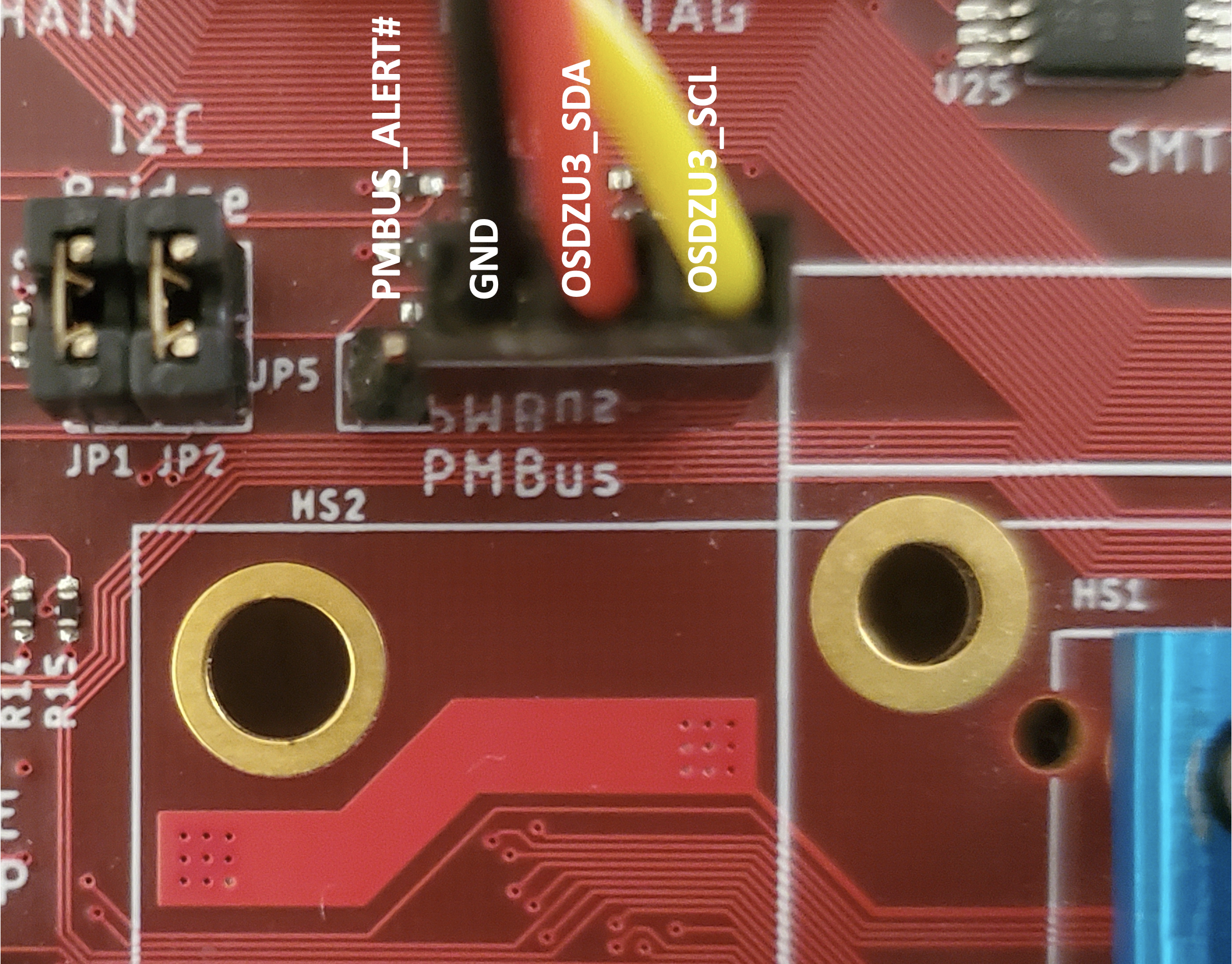
- An OSDZU3 SiP mounted on a Printed Circuit Board (PCB) with PMIC_SCL (BGA ball P27), PMIC_SDA (BGA ball R27), and ground (GND) connected to a 3pin 100mil header. For example, the OSDZU3 Reference Design has a 4 pin PMBus header (J5) as see in the picture below, that can be used to communicate with the PMICs.
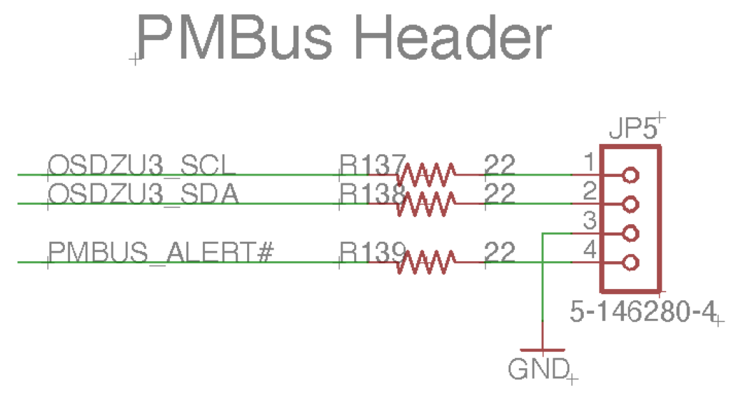

PMBus Header Schematic 

PMBus Header on OSDZU3 Reference Board - Windows Host PC with at least 4 GB RAM
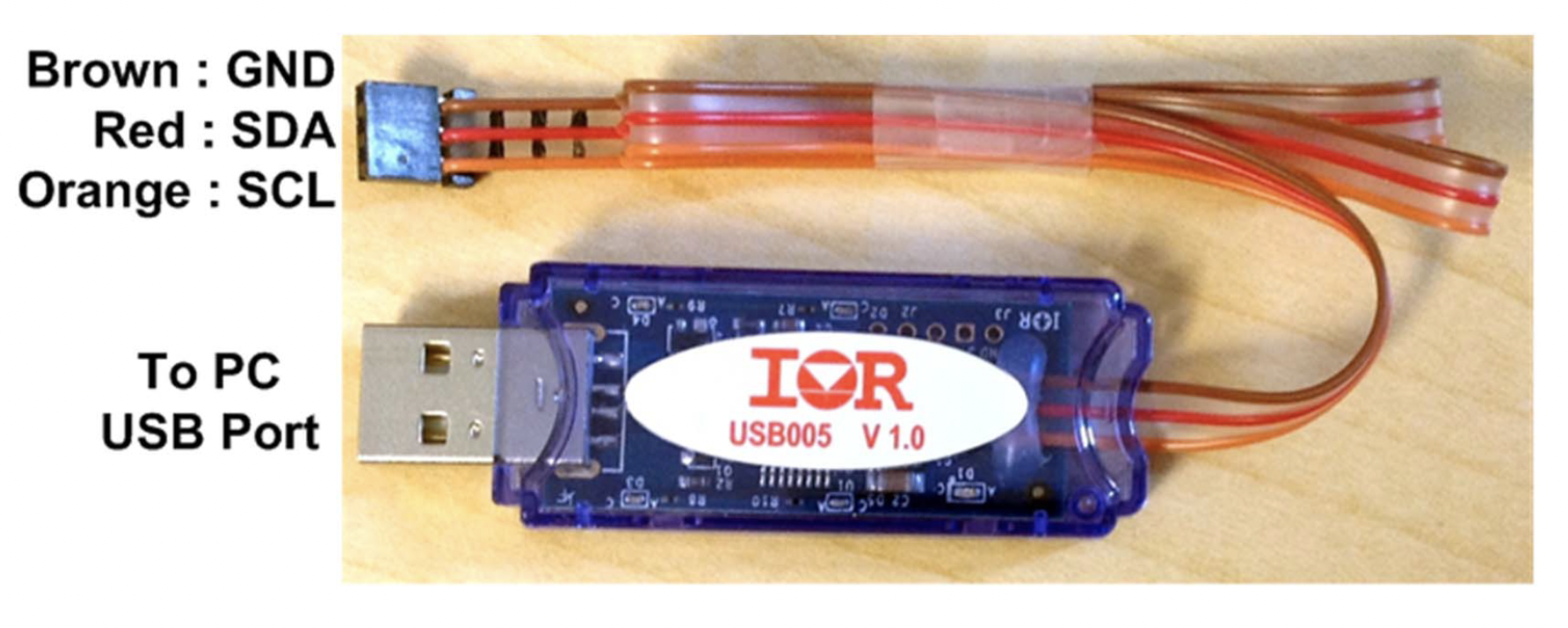
- USB005 adapter


USB005 Adapter
Software
- PowIRCenter Software
- For installation instructions, see sections 2,3 and 4 of Infineon’s User Guide (AN-0035)
- Configuration files (default configuration) of each PMIC from Octavo Systems ( https://octavosystems.com/files/osdzu3-pmic-configuration-settings/) in .txt file format
Initialization
This section will discuss the steps needed to connect to the PowIR software and monitor the PMICs within the OSDZU3.
- To access the PMICs within the OSDZU3 device, certain connections must be made to the SiP as seen in the figure below.
- Both VSUPPLY and +5V_IN power inputs must have a valid 5V input voltage.
- VDDIO must be connected to a 3.3V rail, for example, the on-SiP regulator +3.3V_ON.
- The MTP values should be set to select the appropriate configuration. For example, on OSDZU3 reference design, R1_MTP = 2.32K (MTP segment +3 selected) and R2_MTP = 2.87K (MTP segment +4 selected) (For more information on MTP functionality, see Appendix).
- PWR_EN can either be grounded, all power rails are disabled, or left floating, all power rails are enabled due to internal pull up resistor, when using the PowIR software.
 Note: Below configuration will disable all output rails of OSDZU3’s PMICs. If you will be programming the PMIC, this state should be used to avoid any issues during programming (if you plan to just monitor the PMIC, then you should leave PWR_EN floating). Additionally, when programming the PMIC, you should ensure all other on-board power rails are also disabled to prevent back currents and potential damage to the SiP or the board.
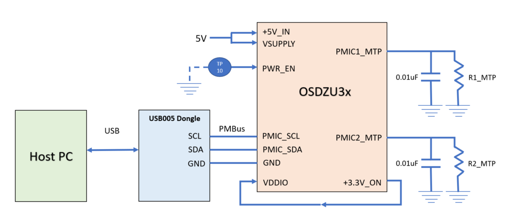

OSDZU3 PMIC Connections
- Provide power to the board.
- Open the PowIRCenter software on Windows Host PC
- Connect USB005 adapter between the Windows Host PC and OSDZU3 SiP as seen above. For example, the PMBus header is brought out to header JP5 on the OSDZU3 reference design. Ensure the SCL/SDA as well as GND wire (black) of the adapter is connected to PMIC_SCL/PMIC_SDA and GND of the OSDZU3 SiP.
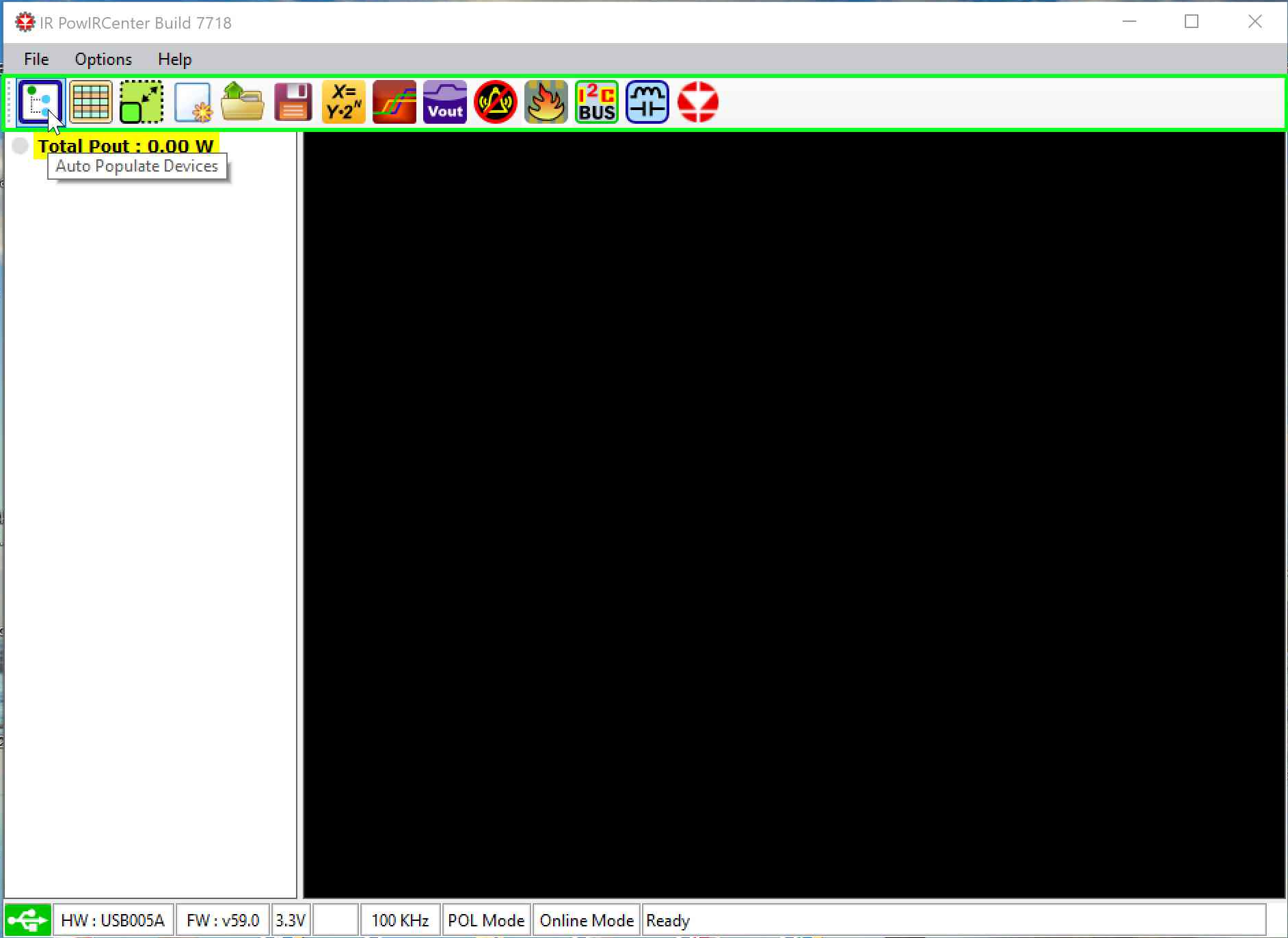
- The USB icon in the bottom left corner of the GUI will turn green once USB005 adapter is detected. Once the adapter is detected, click on the Auto Populate Devices button in the PowIRCenter software.


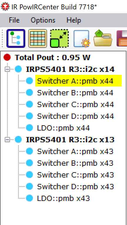
USB Green and Auto Populate - The IRPS5401 PMICs of the OSDZU3 SiP should automatically be detected and shown in the PowIRCenter GUI output as seen in the figure below. The PMIC with address 0x13 corresponds to PMIC1 and the PMIC with address 0x14 corresponds to PMIC2 in the OSDZU3 documentation.
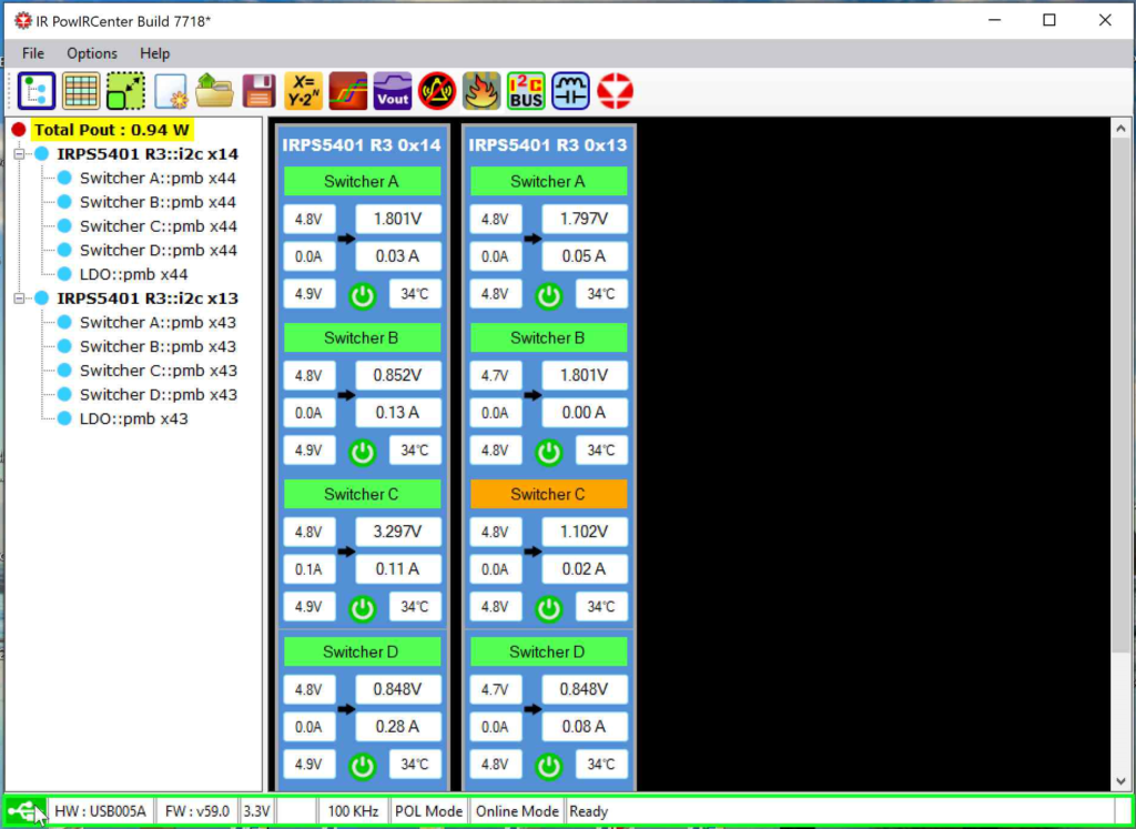

OSDZU3 PMICs Detected By default, the PMICs have the following output voltages:
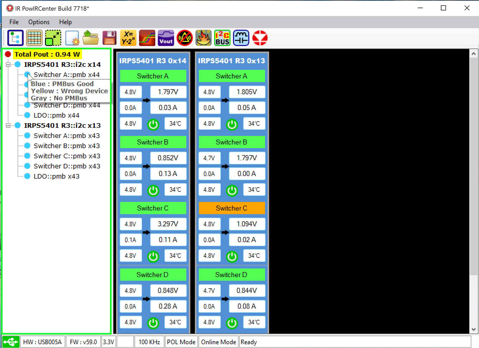
PMIC Address Output Name OSDZU3 Power Output Output Voltage 0x13 VOUT_A – Switcher A VCCAUX 1.80 0x13 VOUT _B – Switcher B PMIC1_B 1.80 0x13 VOUT _C – Switcher C VCCO_PSDDR 1.10 0x13 VOUT _D – Switcher D VCCINT 0.871 0x13 VO_LDO MGTRAVTT 1.80 0x14 VOUT _A – Switcher A VCC_PSAUX 1.80 0x14 VOUT _B – Switcher B VCC_PSINTLP 0.85 0x14 VOUT _C – Switcher C PMIC2_C 3.30 0x14 VOUT _D – Switcher D VCC_PSINTFP 0.914 0x14 VO_LDO VCC_PSPLL 1.20 - The blue circles next to the switcher names indicate a good PMBus connection. A grey circle indicates no PMBus connection. Double check power to the board and USB005 dongle connections if you see grey circles.


Good PMBus Connection


Modifying Specific PMIC Command Values
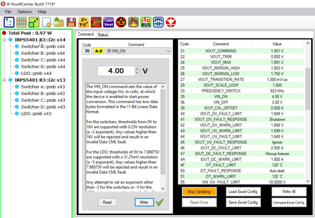
This section will describe the steps to modify specific command values in the PMIC. For example, if you wanted to set the VIN_ON voltage of PMIC 0x14 Switcher A to 4.00V. The steps to modify it are as follows:
- Click on PMIC 0x14 Switcher A under the PMIC Tree View

PMIC 0x14 Switcher A - Under Command window, click on VIN_ON
- Set the voltage to 4.00V (or any other desired value) and click the Write button as shown below. A green tick should appear next to the Write button.

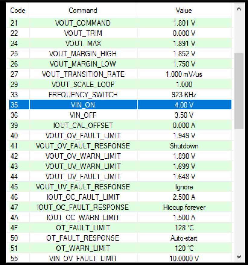
Write Button - The green tick indicates that the updated value has been written to the working registers of the PMIC and the command status window should display the updated value (as shown below). However, the update is NOT written to the PMIC’s MTP (non-volatile memory). Hence, the update will be lost after a power cycle. During every power up sequence, as the PMIC comes out of Power On Reset (POR), it initiates an MTP load cycle, where the contents of the MTP are loaded into the RAM registers. The next five steps need to be followed to program the MTP with the updated value so that it is not reset after a power cycle. See the Appendix to learn more about the memory organization of the PMIC.

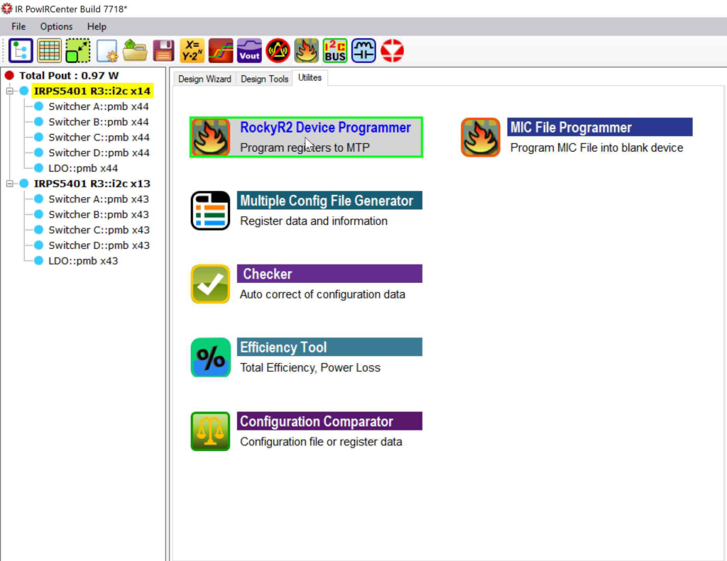
Successful Update - To update the MTP, first select PMIC 0x14 under PMIC Tree View. Then select the Utilities tab, click on RockyR2 Device Programmer.

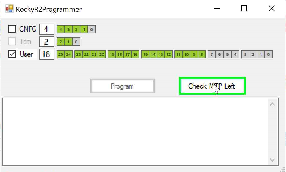
Utilities in the RoxyR2 Programmer - Once the RockyR2 Programmer window appears, click on Check MTP LeftNOTE: The IRPS5401 PMIC can only be written a LIMITED number of times. The MTP count next to the User label (i.e., 18 in figure below) shows the remaining number of times the User Section of the PMIC configuration can be modified. The count reduces by one each time the PMIC configuration is modified. When there are no more available sections to be written, i.e., the count is 0, additional configurations can no longer be added to the PMIC.

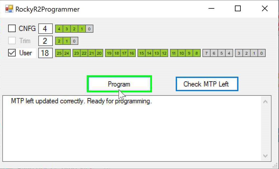
RockyR2 MTP Check - Make sure the User section is selected, then, click on Program to write the updated register values to the User MTP section of the PMIC 0x14.

- The status of programming will be displayed as shown below.
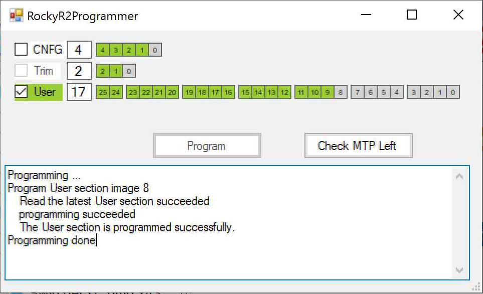

PMIC Programming Status - Once programming is successful, power cycle the board (i.e., remove power, wait for 10s and reapply power), connect to the PMIC, and verify the modified command value again to ensure the updated value was properly written to the PMIC.


Validating and Updating Full PMIC Configuration
This section will describe the steps to:
- Verify the contents of the PMICs against default configuration files provided by Octavo Systems
- Perform full PMIC configuration update or any other custom configuration
- Click on Multi Device Programmer button

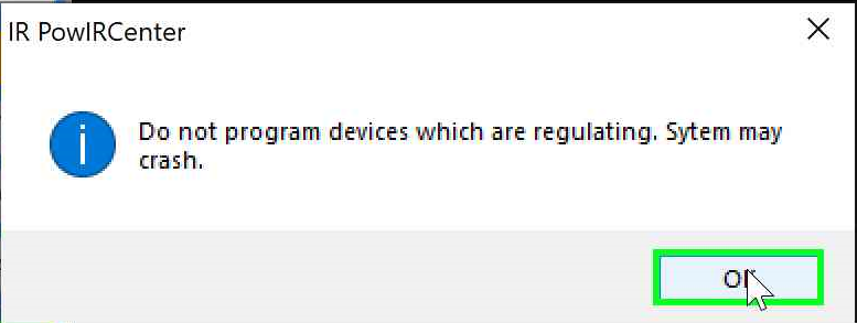
Multidevice Programmer Button - When the following dialog box appears, click OK. Disable all PMIC outputs by

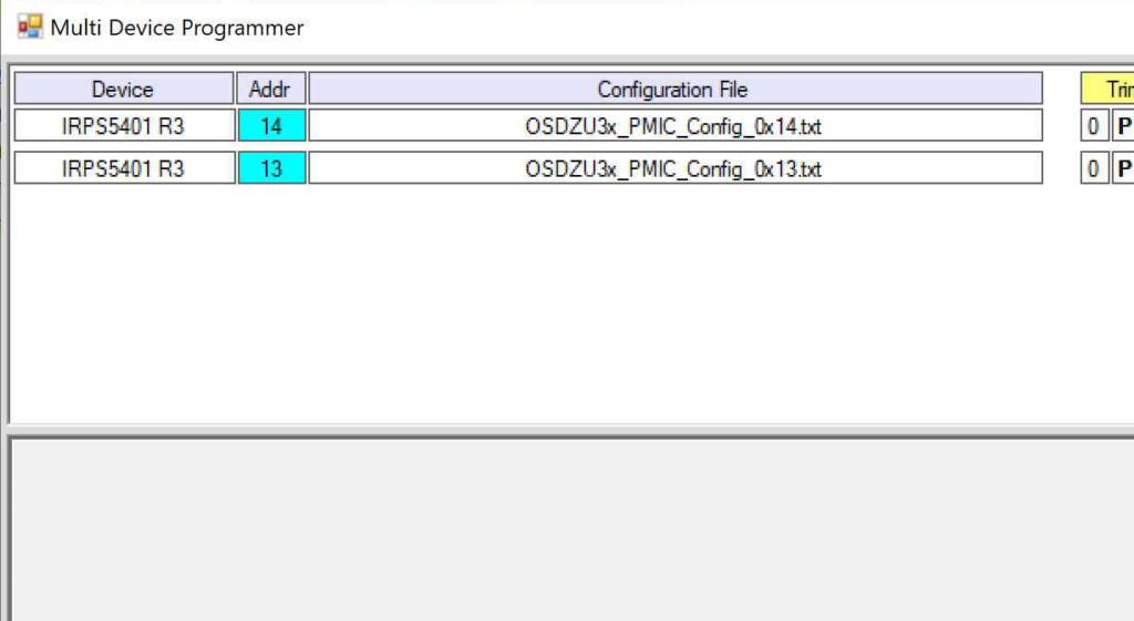
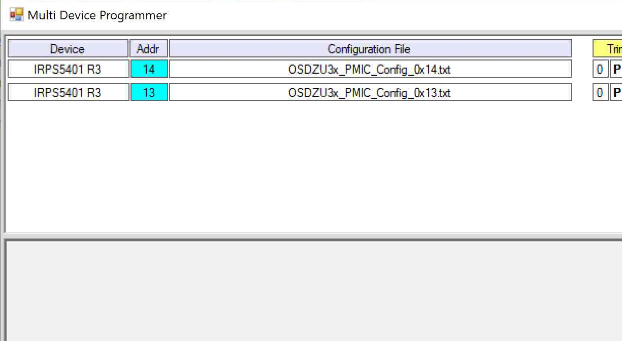
Disable PMIC Outputs - When the Multi Device Programmer window appears, browse the Windows Host PC and choose the appropriate config .txt files for each PMIC from the files provided by Octavo Systems.

Choose Config Files - Click the checkbox next to the User section as shown below.

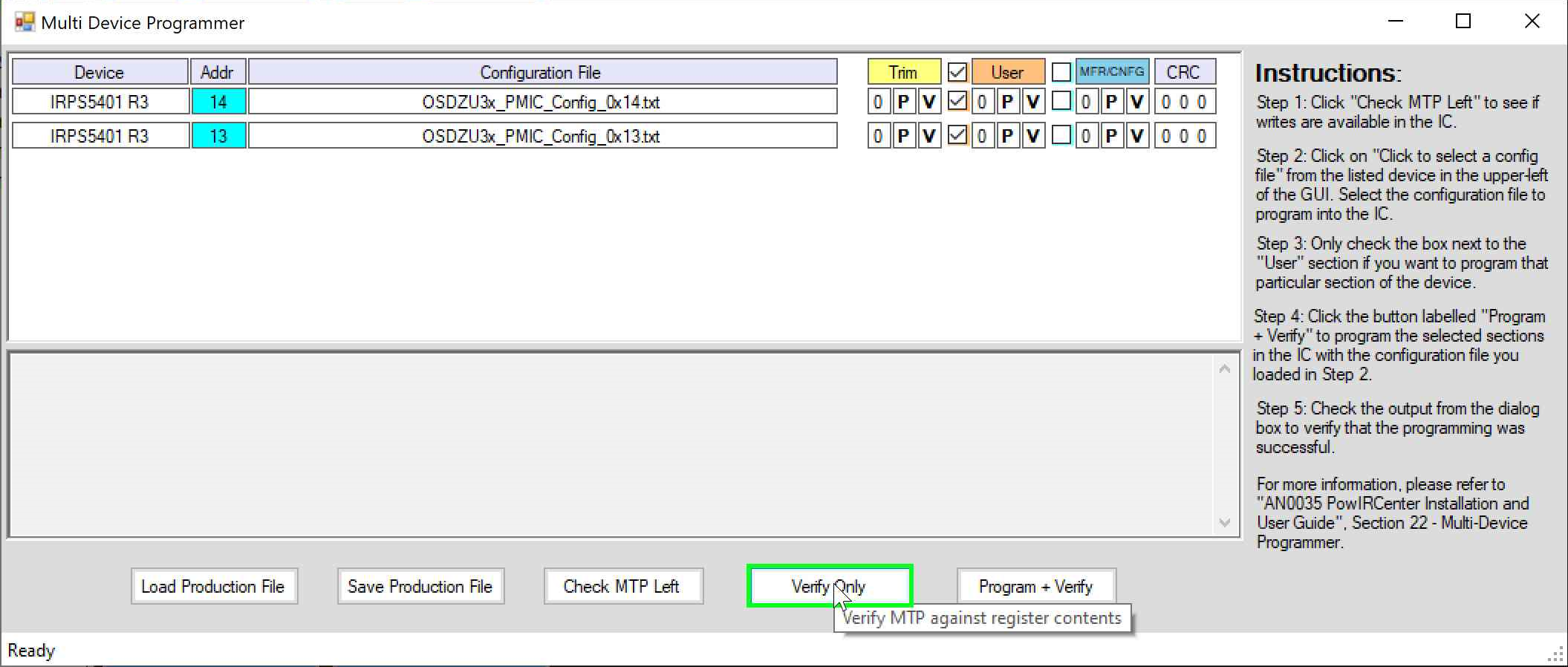
User Section Check Box - To verify the contents of the PMICs against the configuration files provided by Octavo Systems, click on Verify Only.


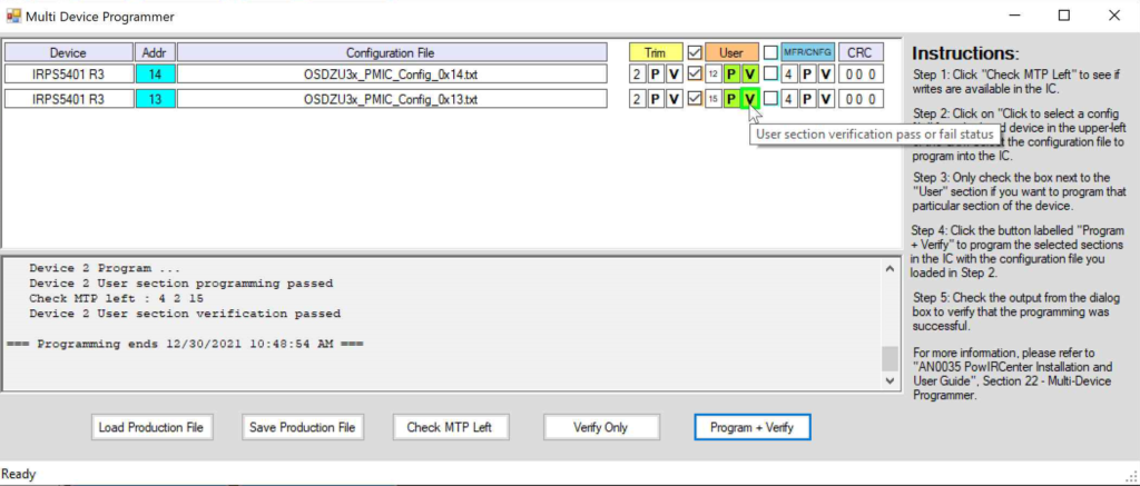
Verify Configuration - If the background of the letter V under User section turns RED, it indicates that the verification failed.

Failed Verifications - You can use the spreadsheets provided by Octavo Systems (link to files given under “Software” section above), which is a human readable version of the .txt configuration files, to manually compare against each of the command values of the PMIC to understand any differences.
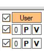
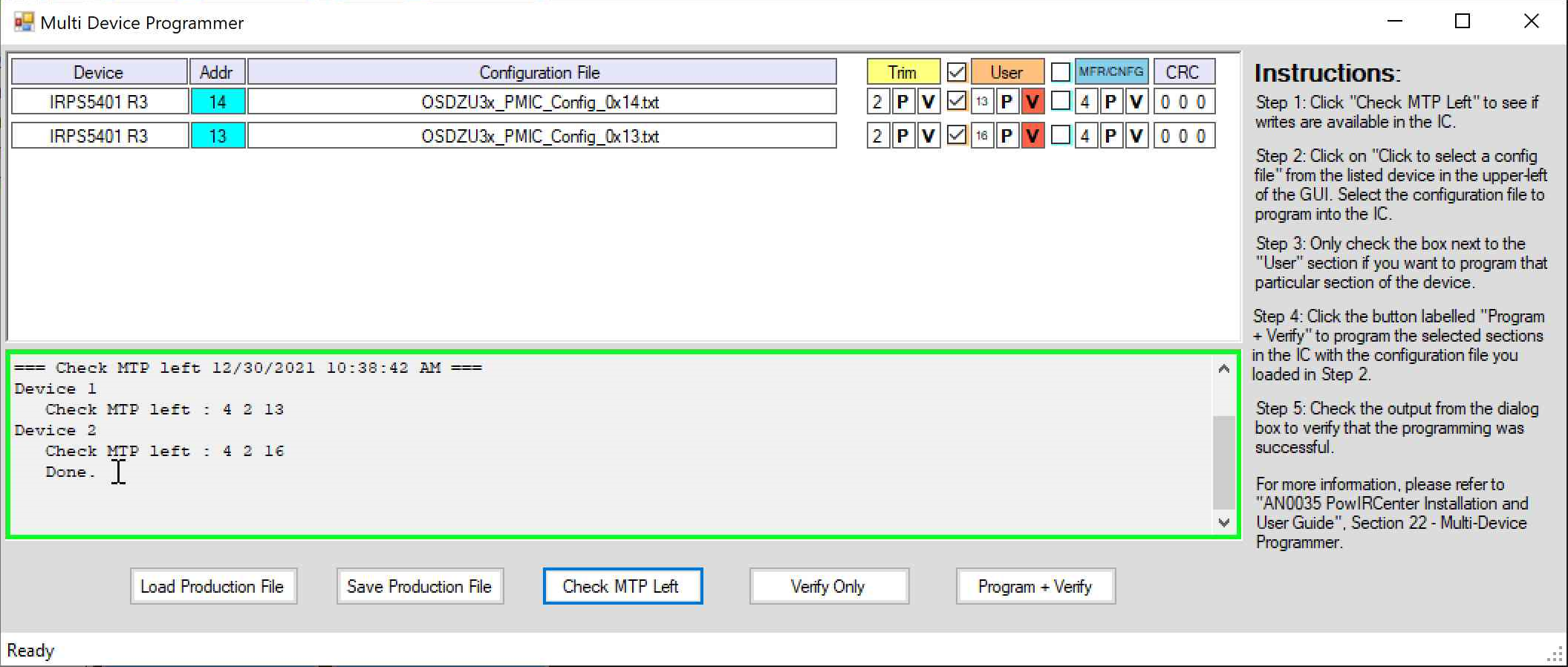
- To program the PMIC back to the defaults from Octavo, first, click on Check MTP Left to get MTP count and see if PMIC permits any more modifications (MTP left count should be greater than 0). The MTP left count for PMIC 0x14 is 13 and PMIC 0x13 is 16 in this example case (see figure below)

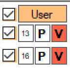
PMIC Configuration Count - Given there are MTP sections available, click on Program + Verify to set the full configuration of both PMICs to the default values. If programming and verification succeeds, the background of P and V for both PMICs should turn green as shown below.

PMIC Configuration Programming Success


Appendix
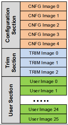
IRPS5401 PMIC MTP (Multiple Times Programmable) Memory Organization
Each of OSDZU3’s two PMICs contain three sections of “One Time Programmable” (OTP) segments (see figure below):
- Configuration Section – stores device specific information and allows 5 writes
- Trim Section – contains the device calibration data which is programmed at the factory and allows no writes
- User Section – contains the PMIC configuration data, such as the output voltage setting for various switchers and LDOs, input voltage/current limits, output voltage/current limits, under/over voltage limits, output read registers, etc. and allows 26 writes
The IRPS5401 PMIC contains several OTP images or slots, that can each be written once. However, because the PMIC will only load the OTP image from the highest programmed slot, the PMIC configuration can be changed multiple times. Therefore, the OTP configuration memory is also referred to as a “Multiple-Times Programmable” (MTP) memory space.
PMICx_MTP Pins
In the OTP Config Registers (Address 0x0), the cnfg_nvm_prog_max field can be used to control the functionality of the MTP pins. By default, in the OSDZU3 parts, the value is 0x0, which disables the feature. When the feature is disabled, the MTP pins are ignored, and the OTP image loaded during boot is the highest programmed image within the MTP memory.
The cnfg_nvm_prog_max may be programed so that the MTP pins can be used to select the OTP image that is loaded during boot. The table below shows the MTP segment that will be selected with a given resistor value connected to the PMICx_MTP pin. The resistor must be connected to the AGND pin and bypassed with a 0.01uF X7R type multi-layer ceramic capacitor.
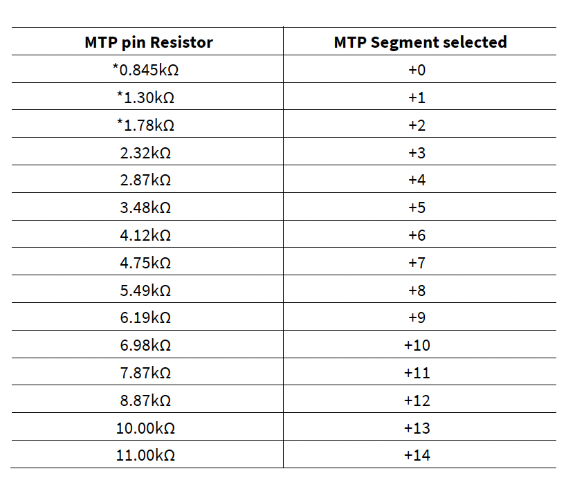
If the MTP feature is used by Octavo Systems, cnfg_nvm_prog_max will be programmed with a value of 0x4. The default configuration for PMIC1 (Address 0x13) will be located in MTP Segment +3 and the default configuration for PMIC2 (Address 0x14) will be located in MTP Segment +4. Therefore, it is recommended to future proof a design that the MTP pin for PMIC1 be connected to a 2.32k resistor and the MTP pin for PMIC2 be connected to a 2.87k resistor as described in Section 3. If the MTP pins are used to select the OTP value, the PMICs can still be re-configured by changing cnfg_nvm_prog_max back to zero and programming an updated User Image into the OTP memory.
References
- IRPS5401 PMIC datasheet – https://www.infineon.com/dgdl/Infineon-IRPS5401M-DataSheet-v02_06-EN.pdf
- PowIRCenter Installation and User Guide – https://www.infineon.com/dgdl/an-0035.pdf
- IRPS5401 Register Map – https://www.infineon.com/dgdl/Infineon-DC-DC_POL_IRPS5401_Register_Map-AdditionalTechnicalInformation-v01_03-EN.pdf
- IRPS5401 command set – https://www.infineon.com/dgdl/Infineon-DC-DC_IPOL_IRPS5401_PMBus_Command_Set-AdditionalTechnicalInformation-v01_03-EN.pdf
- Rocky Programming Guide For IRPS5401 – https://www.infineon.com/dgdl/Infineon-DC-DC_POL_IRPS5401_Programming_Guide-AdditionalTechnicalInformation-v01_08-EN.pdf
Revision History
Stay up to date on changes to this app note and other information from Octavo Systems by signing up for our newsletter.
"*" indicates required fields
| Revision Number | Revision Date | Changes | Author |
| 1 | 02/11/2022 | Initial Revision | Eshtaartha Basu |
| 2 | 09/07/2023 | Production Release | Eshtaartha Basu |
