OSDZU3 Power Application Note
Published On: September, 19, 2023 By: Eshtaartha Basu | Updated: November 1, 2023 by Greg Sheridan
This application note is intended for engineers to understand the power management system of the OSDZU3 family of devices. It is also intended to aid in power budgeting for systems using a OSDZU3 device. It provides an overview of the power management system inside the OSDZU3 and runs through an example application power budgeting procedure using the OSDZU3-REF board.

Table of Contents
OSDZU3 Power System Introduction
The OSDZU3 contains two IRPS5401 Power Management Integrated Circuits (PMICs), two Low Drop-Out (LDO) regulators and associated passives for power management. The PMICs are responsible for powering the AMD XCZU3 MPSoC, LPDDR4, QSPI Flash, EEPROM, the two LDOs as well as provide output power for other system needs. They provide configurable power-up and power-down sequencing required by the processor and monitor the processor input voltage levels. Each of the two PMICs contains 4 Switching Regulators and 1 LDO. The power management system of OSDZU3 accepts 4.5V to 5.5V input by default. It is possible to adjust the PMIC settings using the Infineon PowIRCenter software suite. More information on updating the PMIC settings can be found in the PMIC Programming Guide.
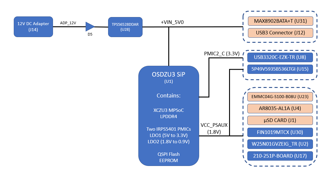
The following figure shows the power system of the OSDZU3 including internal connections between the PMIC and various power domains of the processor.
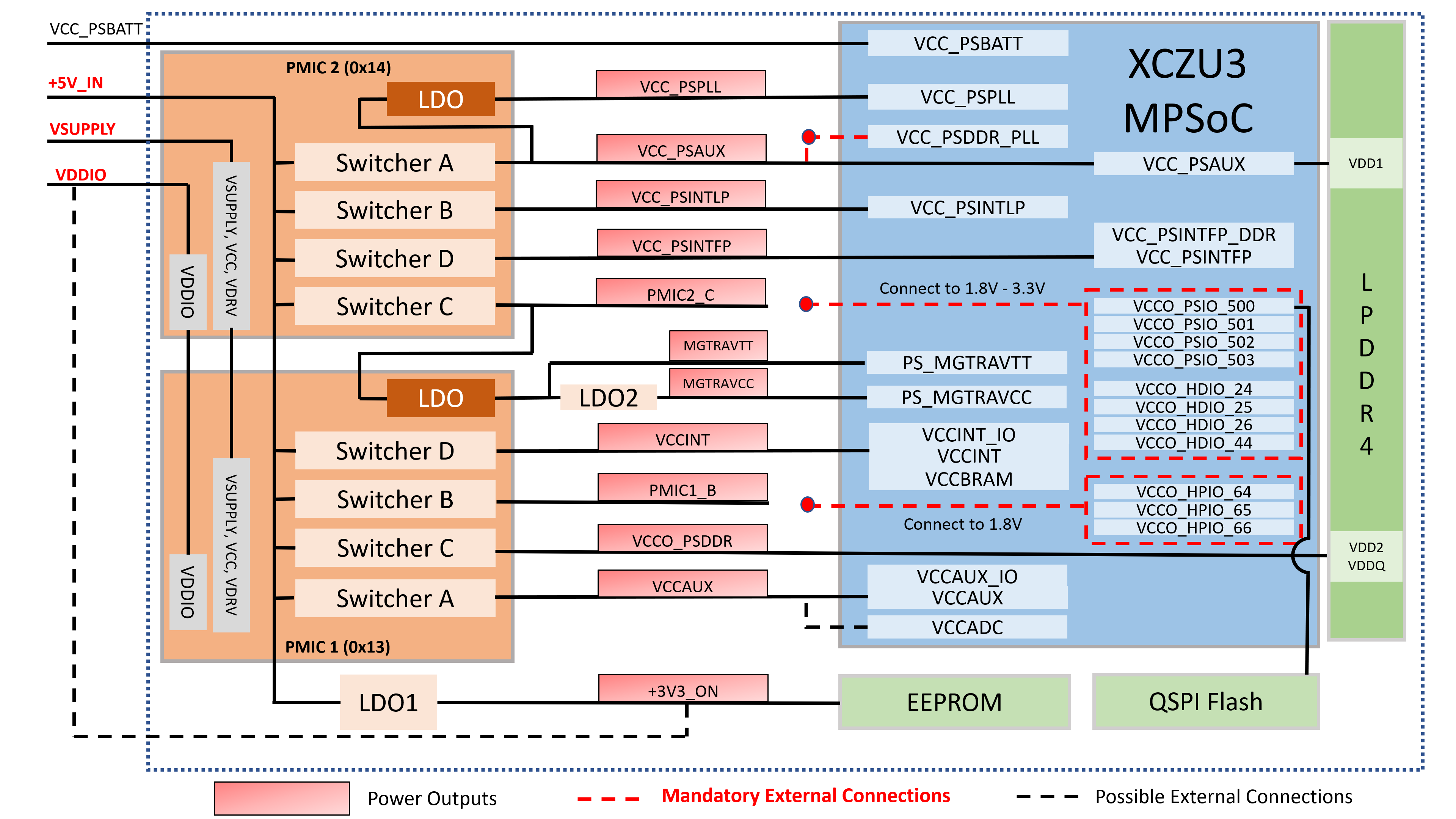
The OSDZU3 Output Rails table shows the default output voltage levels of each of the voltage sources. Each of the output voltages can be changed dynamically using I2C / PMBUS commands when the PMIC is in active mode.
The OSDZU3 Recommended External Power IO Connections table shows recommended external power IO connections for OSDZU3.
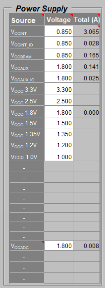
| Voltage Source | OSDZU3 Voltage rail | Voltage (V) | For External Use? |
|---|---|---|---|
| PMIC 2 LDO** | VCC_PSPLL | 1.2 | NO |
| PMIC 2 Switcher A** | VCC_PSAUX | 1.801 | YES |
| PMIC 2 Switcher B** | VCC_PSINTLP | 0.852 | NO |
| PMIC 2 Switcher C** | PMIC2_C | 3.301 (default), user adjustable | YES |
| PMIC 2 Switcher D** | VCC_PSINTFP | 0.914 | NO |
| PMIC 1 LDO* | +MGTRAVTT | 1.8 | NO |
| PMIC 1 Switcher A* | VCCAUX | 1.801 | YES |
| PMIC 1 Switcher B* | PMIC1_B | 1.801 (default), user adjustable | YES |
| PMIC 1 Switcher C* | VCCO_PSDDR | 1.102 | NO |
| PMIC 1 Switcher D* | VCCINT | 0.871 | NO |
| LDO2 | +MGTRAVCC | 0.9 | NO |
| LDO1 | +3V3_ON | 3.3 | NO |
* PMIC 1 I2C address = 0x13
** PMIC 2 I2C address = 0x14
| OSDZU3 Power Inputs (1) | Recommended External Connections |
|---|---|
| +5V_IN | Requires 4.5V – 5.5V power source capable of 1.5A in-rush current |
| VSUPPLY | Requires 4.5V – 5.5V power source |
| VCC_PSDDR_PLL input | VCC_PSAUX output |
| VDDIO input | 3.3V_ON output |
(1) External bulk capacitors and ferrite beads may be required for some inputs. See OSDZU3 Schematic Checklist for more detailed info.
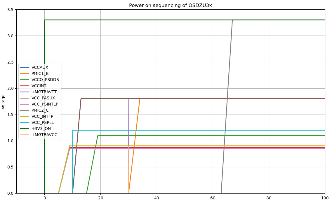
The below table and figure show the rise times, fall times and power-up sequencing for all the power rails. More information can be found in the PMIC Programming Guide.
| OSDZU3 rail | Voltage (V) | Ton_delay(ms) | Ton_rise(ms) | Toff_delay(ms) | Toff_fall(ms) |
|---|---|---|---|---|---|
| VCC_PSPLL | 1.2 | 10 | 0 | 0 | 0 |
| VCC_PSAUX | 1.801 | 10 | 3 | 0 | 1 |
| VCC_PSINTLP | 0.852 | 5 | 4 | 0 | 1 |
| PMIC2_C | 3.301 | 63 | 4 | 0 | 1 |
| VCC_PSINTFP | 0.914 | 5 | 4 | 0 | 1 |
| +MGTRAVTT | 1.8 | 30 | 0 | 0 | 0 |
| VCCAUX | 1.801 | 10 | 3 | 0 | 1 |
| PMIC1_B | 1.801 | 30 | 4 | 0 | 1 |
| VCCO_PSDDR | 1.102 | 15 | 4 | 0 | 1 |
| VCCINT | 0.871 | 5 | 4 | 0 | 1 |
| +MGTRAVCC | 0.9 | 30 | 0 | 0 | 0 |
| +3V3_ON | 3.3 | 0 | 0 | – | – |
Power Design Considerations – Inrush Current
Inrush current is the maximum instantaneous input current drawn by a system during power up. This instantaneous current can be higher than the steady state current the system consumes.
For the OSDZU3 family, the IRPS5401 PMICs manage the power rails to the processor, other peripherals, and output power rails of the SiP. The following figure shows an example of a power up fault where the input power rail is unable to sustain the specified inrush current requirements leading to momentary dips in input voltage (highlighted in red).
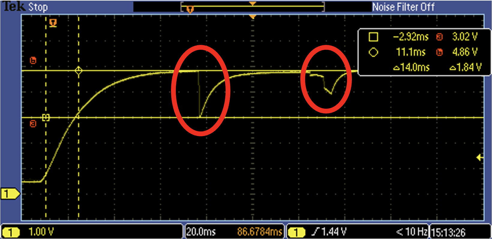
Two factors that affect inrush behavior are the input power supply capacity and the bypass capacitance. To mitigate a fault condition, the load current rating of the power supply used to power the system must exceed the inrush current of the system. Although inrush current is specific to a system and can vary, typical inrush current measurements for the OSDZU3 family is given in the below table.
| Power Input | Typical Inrush Current (mA) |
|---|---|
| +5V_IN supplied with 5V | 1500 |
In addition to the current capacity of power source, external bypass capacitances on the power rails that power the processor and other downstream components will help stabilize the rails during operation. For the list of recommended external capacitances and internal bulk capacitances already integrated within the SiP, see Capacitors section of the OSDZU3 Datasheet. Also see OSDZU3 Schematic Checklist for design recommendations.
Power Budgeting: How to Approach it?
Octavo Systems recommends making a power budget for your product/design at the beginning of the project. Good power budgeting contributes to circuit robustness, increased product life and reduced cost of the product.
Step 1: Creating a Power Diagram
The first step in making a power budget is to create a power block diagram that shows all the power paths of the system, starting with all the available power sources for the system. For the OSDZU3, this would include the external power supply inputs that power the OSDZU3 as well as OSDZU3 output power rails that are described in the Table – PMIC voltage output requirements for OSDZU3 of the OSDZU3 datasheet.
There are four available external output power rails on the OSDZU3:
- PMIC1_B (default 1.8V, user adjustable) *
- PMIC2_C (default 3.3V, user adjustable) *
- VCC_PSAUX (1.8V, fixed)
- VCCAUX (1.8V, fixed)*
*User adjustable, see PMIC Programming Guide for more information on configuring output rails of the OSDZU3.
Next, add the power consuming components to the diagram and connect each to the appropriate power rail. The connection should be based on the required input voltage level for the component and the current capacity of the power rail.
For example, the power block diagram for the OSDZU3-REF board that includes on-board components that draw at least 50mW of power is shown in the figure below.

The diagram not only shows the power rails for a particular component but also lists all the components that are being powered by a power rail. In addition to helping with the power budgeting, this allows you to identify power issues early in the design process and make necessary adjustments.
4.2 Step 2: Creating a Power Budget
The next step involves creating a power budget to estimate power consumption of the SiP, each secondary (on-board) component and thus the total power consumption of the board.
There are several challenges involved in accurately estimating the power consumption of each component. For example, it is difficult to estimate how much power the XCZU3 MPSoC and the LPDDR4 memory consume since it is highly application specific. However, it is straightforward to get typical and maximum power consumption of secondary components such as µSD card, eMMC, Ethernet PHY, etc. from their respective datasheets. Hence, it would be more convenient to divide the power budgeting process into three sub steps:
- Step 2a: Estimate power consumption of XCZU3 MPSoC and LPDDR under common use cases
- Step 2b*: Estimate power consumption of secondary components under typical and high use
- Step 2c*: Combine the estimates of Step 2a and 2b

Step 2a-1: Estimate Power Consumption of XCZU3 MPSoC
The AMD XCZU3 MPSoC integrates a large array of customizable logic, memory, processor, and many peripherals. As a result, power consumption depends on multiple factors such as device usage %, thermal management (see Further Reading section for more info), clock frequency, enable rate, toggle rate, etc.
AMD provides a power estimation tool, Xilinx Power Estimation (XPE) spreadsheet that can calculate the internal power consumption of XCZU3 MPSoC including its individual power domains. You can download the latest version here (AMD registration may be necessary). XPE has been used for the XCZU3 power estimations in this app note.
XPE is generally used for power estimation of the Programmable Logic (PL) before implementation of the design in Vivado. However, Vivado’s power report post-implementation can also be imported to XPE for a more accurate estimate. XPE can also be used for Processing System (PS) power estimation.
Similar to AMD’s XPE spreadsheet, Micron also provides a spreadsheet to estimate LPDDR4 power consumption that can be used to get a good estimate. You can download the latest version here (Restricted access – Micron registration may be ).
XPE 2023.1.2 and Vivado 2023.1 were used to arrive at the estimations presented in this app note.
The following sections will explore how to use AMD’s XPE and Micron’s LPDDR4 spreadsheets to estimate the power used by the XCZU3 MPSoC (both PL and PS) and the LPDDR4 memory. A few example use cases of the PL and PS with their power estimates will also be presented.
XPE PL Power Estimation
XPE PL Power Estimation can be done using one of the following 2 methods:
- Method 1: XPE PL Power Estimation Pre-Implementation in Vivado – Less Accurate
- Use this method for a preliminary estimate if you do not have a design implemented in Vivado. This estimate will be less accurate and should only be used to arrive at a rough ballpark figure.
- Method 2: XPE PL Power Estimation Post-Implementation in Vivado – More Accurate
- Use this method if you already have a design implemented in Vivado. This estimate will be more accurate compared to previous method since more of the design parameters are known.
Both methods are described below.
Method 1: XPE PL Power Estimation Pre-Implementation
- Open XPE.
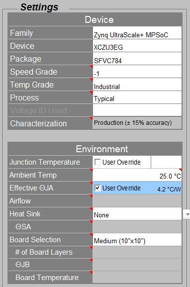
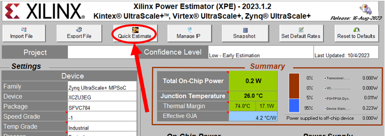
- Choose the correct device and environment settings in the Summary sheet. For the OSDZU3EG1-2G-Ixx, please use the Device settings shown the following figure. Environment settings can be modified to fit your application. The Speed Grade and Temp Grade will vary depending on what version of the device you are using.

OSDZU3 Device and Environment Settings - Click on Quick Estimate in the Summary page as shown in the figure below.

Quick Estimate Button - Enter design parameters of your design as accurately as possible. An example configuration is shown in the following figure:
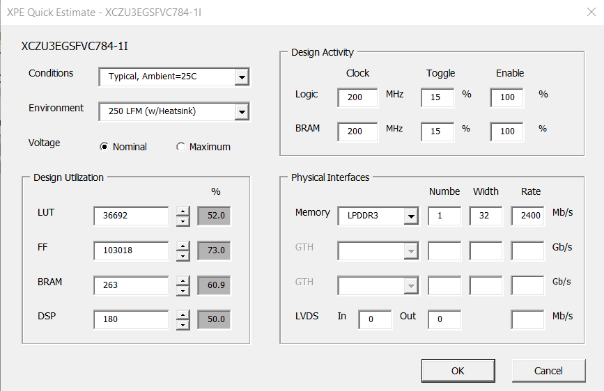

Quick Estimate Window Note: XPE does not support LPDDR4 memory power estimates as of Sep 2023. As a result, in the above picture, LPDDR3 memory parameters have been used which are close to LPDDR4 memory parameters. Support for LPDDR4 memory may be added in a future release as suggest by AMD support team here – https://support.xilinx.com/s/article/76108?language=en_US - Once the Quick Estimate window finishes, tune the parameters in each of the IP sheets (Logic, BRAM, DSP, etc) to match your design specification.
- Check the summary page for the Power Estimate based on the provided information:
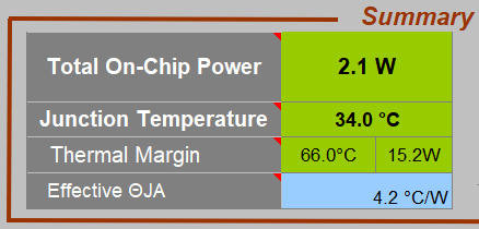

Quick Total Power Estimate for Example Input Parameters
Method 2: XPE PL Power Estimation Post-Implementation
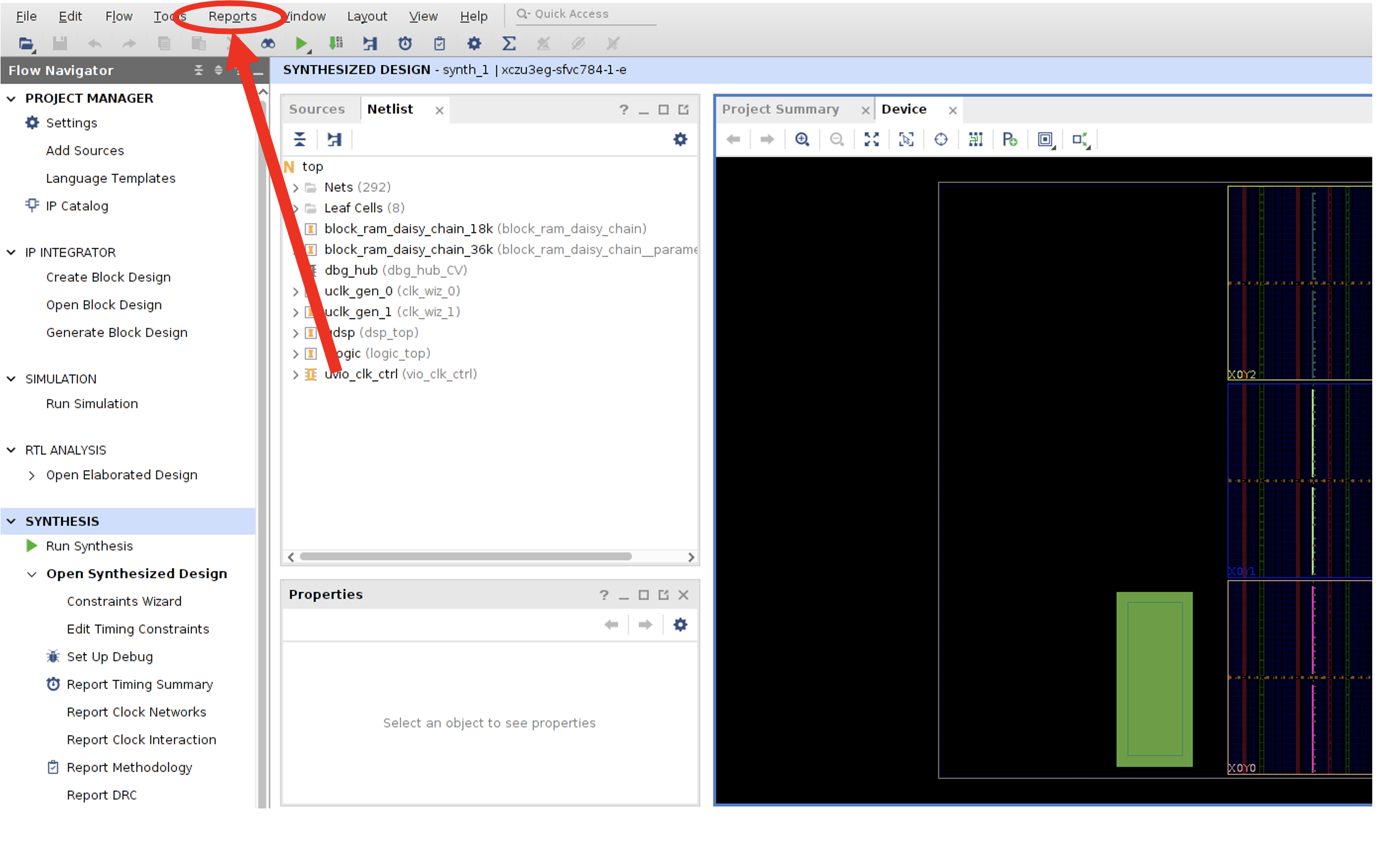
- Open your Vivado project that contains your Implemented Design.
- Click on “Open Implemented Design” under Flow Navigator
- Click on Reports > Report Power as shown in following figure.
- In the Report Power window, under Environment, Power Supply and Switching tabs, ensure all the settings accurately reflect your design.


Reports Tab - Under the Output tab, select Output XPE file, choose file export location and click on OK.
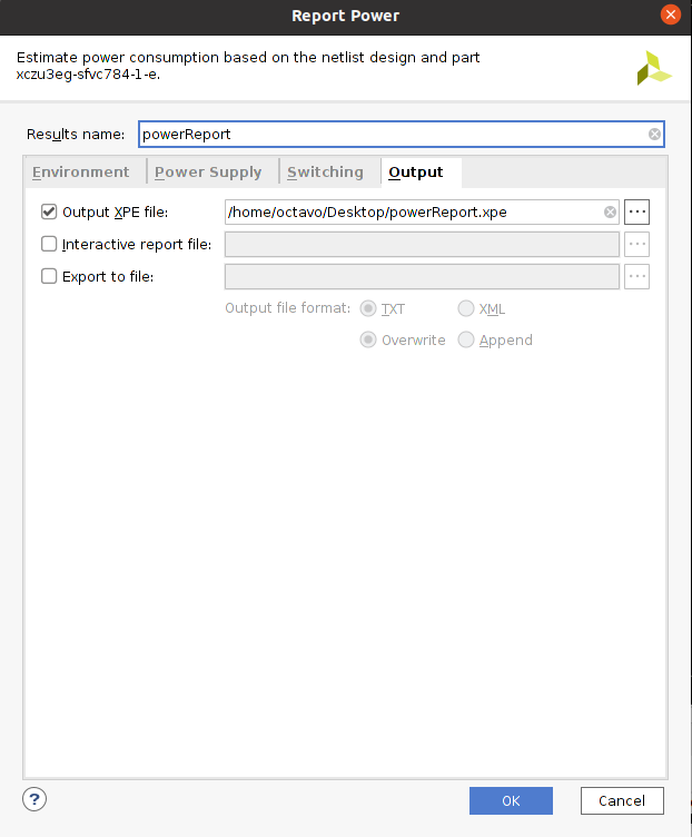

Report Power Window - Open XPE. Select Import File. Choose the exported .xpe file from Vivado.
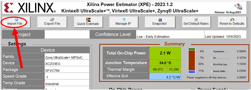

Import file button 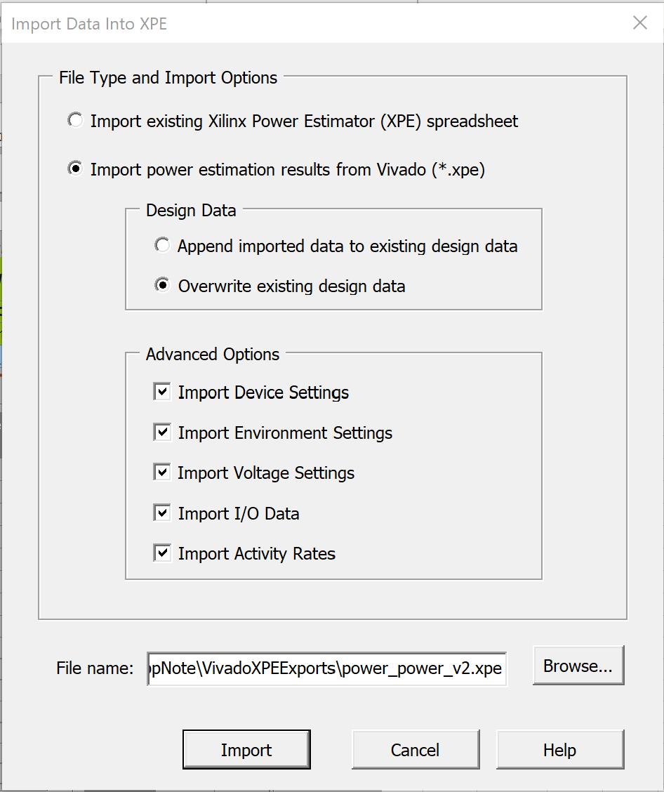

Import File Window - XPE will import the design parameters from the .xpe file and provide a more accurate power estimate in the Summary sheet.
XPE PS Power Estimation
- Open XPE
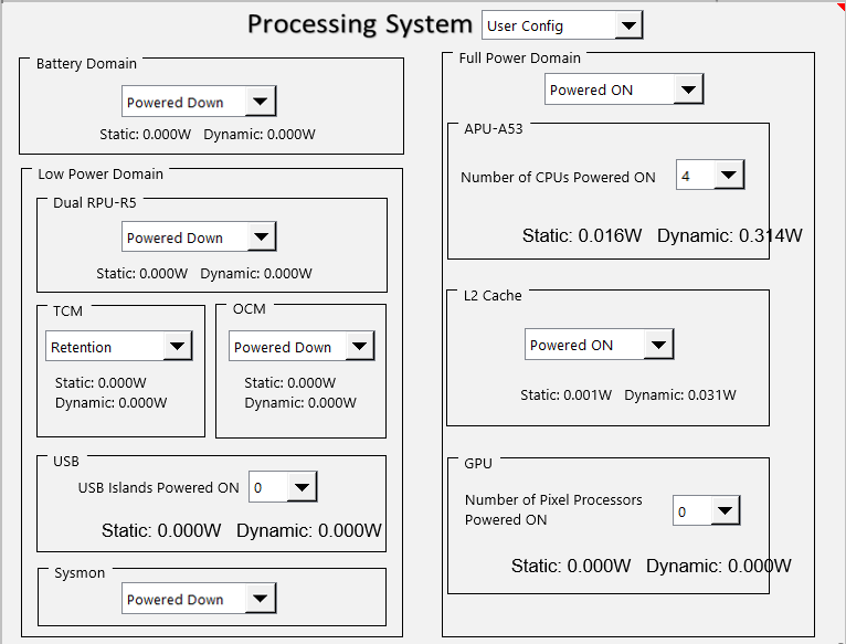
- Under the PS tab, set the parameters of the Processing System (PS) to match your application. An example configuration is shown in the next 3 figures.
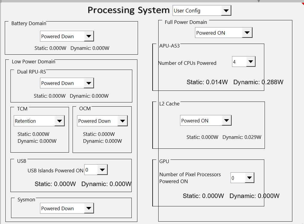

Processing System Config 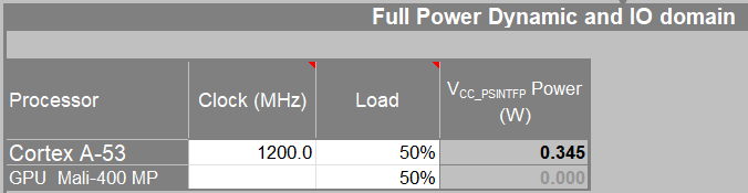

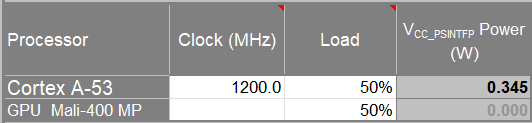
Example Cortex A-53 Config in XPE 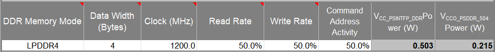

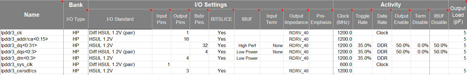
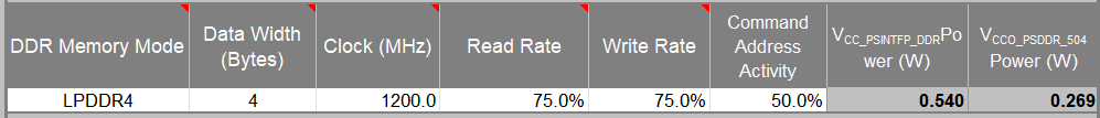
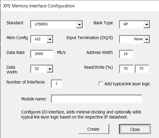
Example LPDDR4 Config in XPE - To estimate power for XCZU3 DRAM IO interface, in IO sheet of XPE, click on “Add Memory Interface” to set DRAM parameters of your design. An example configuration for OSDZU3 DRAM with the following parameters is shown in 2 following 2 figures.
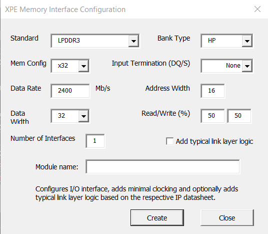

XPE Example Memory IP Configuration Inputs 

Example XPE Memory IP Configuration
PL and PS Example Use Cases
The power consumption of the PL and PS of OSDZU3 are application specific and could vary over a broad range. To provide some reference points on ZU3 power consumption under example scenarios, the following estimates have been compiled. In each example, estimated resource utilization and corresponding power/current estimates are provided. The resource usage estimates were obtained from Vivado (post-implementation) and power/current estimates come from XPE (using the procedure described in sections above).
Case 1: Programmable Logic (PL) – Moderate Utilization
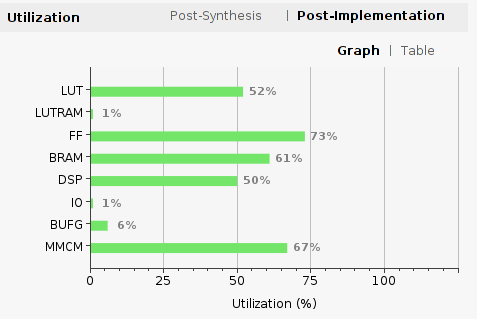
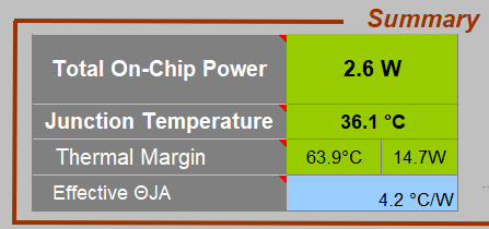
For a PL application with moderate resource utilization as shown in the PL Resource Utilization for Case 1 figure, clock rate of 200MHz, and toggle rate of 15%, the estimated power consumption by XCZU3 is 2.6W and estimated total VCCINT current is 2.7A as shown in the Total XCZU3 Power Estimate for Case 1 and XCZU3 PL Current Estimates for Case 1 figures.
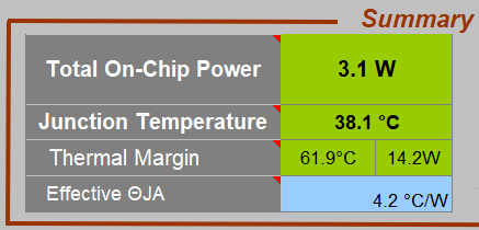
Case 2: Programmable Logic (PL) – High Utilization
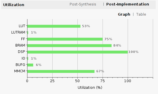
For a PL application with high resource utilization as shown in the PL Resource Utilization for Case 2 figure, a clock rate of 200MHz, and a toggle rate of 15%, the estimated power consumption by XCZU3 is 3.1W and estimated VCCINT current is 3.26A as shown in the Total XCZU3 Power Estimate for Case 2 and XCZU3 PL Current Estimates for Case 2 figures.
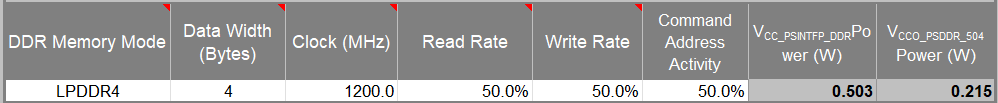
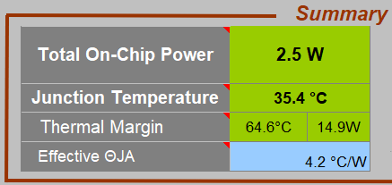
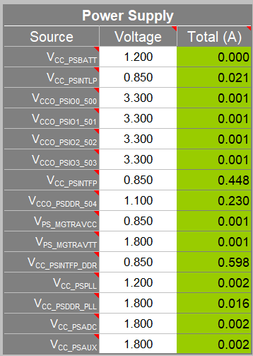
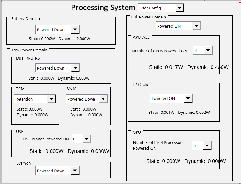
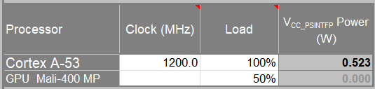
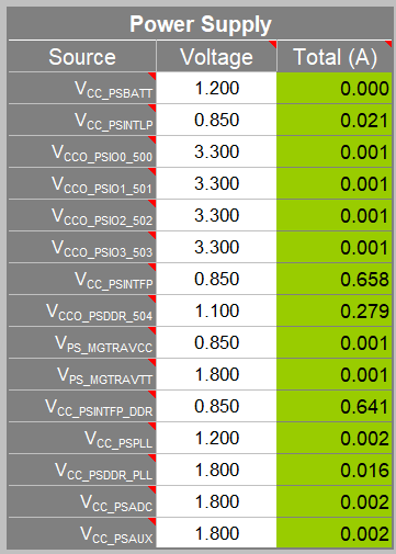
Case 3: Processing System (PS) – Moderate CPU Load
For a PS application with moderate CPU utilization as shown in the next 4 figures the estimated power consumption by the PS of XCZU3 is 2.5W. Estimated VCC_PSINTFP current is 1.05A as shown in Total XCZU3 Power Estimate for Case 3 and XCZU3 PS Current Estimates for Case 3 figures.

Case 4: Processing System (PS) – High CPU Load
For a PS application with high CPU utilization as shown in the next 4 images the estimated power consumption by XCZU3 is 2.9W. Estimated VCC_PSINTFP current is 1.3A as shown in the Total XCZU3 Power Estimate for Case 4 and XCZU3 PS Current Estimates for Case 4 figures.

Step 2a-2: DRAM Power Estimation
Similar to AMD’s XPE spreadsheet, Micron provides a spreadsheet to estimate LPDDR4 power consumption. The exact power consumption depends on the part number and use case, but the spreadsheet can provide an approximate power estimation. A brief use case of the spreadsheet is shown below.
- Download the spreadsheet available for the LPDDR4 memory from Micron’s website (Restricted access – Micron registration may be necessary).
- Input SDRAM configuration inputs under “Device Config”. The table below shows inputs specific to LPDDR4 memory used in OSDZU3EG1-2G-BFx.
OSDZU3EG1-2G-BFx LPDDR4 Device Config Parameter Condition VDD1
ValueVDD2
ValueVDDQ
ValueUnits Number of DQ per DRAM 16 n/a CA ODT 0:ODT disabled 1:ODT enabled, 1rankPKG 2:ODT enabled, 2rankPKG, TermRank 3:ODT enabled, 2rankPKG, NonTermRank 0 IDD0 Maximum active precharge current 3.7 52 0.75 mA IDD2P Maximum precharge power-down standby current 1.2 3.6 0.75 mA IDD2PS Maximum precharge power-down standby current, clock stopped 1.2 3.6 0.75 mA IDD2N Maximum precharge standby current 1.4 34 0.75 mA IDD3P Maximum active power-down standby current 1.2 16 0.75 mA IDD3PS Maximum active power-down standby current, clock stopped 1.2 16 0.75 mA IDD3N Maximum active standby current 1.7 38 0.75 mA IDD4R Maximum read burst current 3.8 380 76.8 mA IDD4W Maximum write burst current 2.3 320 0.75 mA IDD5 Maximum burst refresh current 14 120 0.75 mA IDD6 Maximum burst refresh current 1.5 5 0.75 mA clock tCK used for current measurements (see current notes) 0.468 ns tRRD Minimum activate-to-activate timing (different bank) 10 ns tRC Minimum activate-to-activate timing (same bank) 60 ns tRAS tRAS used for IDD0 calculation 42 ns tRFC,MIN Minimum refresh-to-refresh cycle time 280 ns tREFI Average periodic refresh cycle time 3.9 µs tCK, MIN Minimum tCK cycle rate 0.468 ns tCK, MAX Maximum tCK cycle rate 100 ns - Input DRAM usage conditions under “Usage Conditions”. These inputs vary based on the use case. The following tables show inputs for typical and worst case power consumption of the LPDDR4.
Typical Case Usage Conditions Parameter Value System VDD (VDD1/VDD2/VDDQ)* 1.8 1.1 1.1 System Clock Frequency (MHz) 1200 Burst Length 16 Is DQ terminated during READs ? 1 If terminated, SoC DQ term during READs 60 ohm VOH during READs 0.5 VDDQ Is DQ terminated during WRITEs ? 1 If terminated, LPDDR4 DQ term during WRITEs 80 ohm Page Hit Rate 0.45 The percentage of clock cycles which are outputting read data from the DRAM 0.36 The percentage of clock cycles which are inputting write data to the DRAM 0.12 Percentage of time that the DRAM is in the idle state (all banks precharged). 0.4 The percentage of the idle time for which the device is in power-down (CKE LOW). 0.1 The percentage of the idle time for which the device is in self-refresh. 0.8 Percentage of the total active time for which CKE is held LOW. 0.1 * Internally, VDD1 of DRAM is supplied by VCC_PSAUX. VDD2 and VDDQ supplied by VCCO_PSDDR.
Worst Case Usage Conditions Parameter Value System VDD (VDD1/VDD2/VDDQ)* 1.8 1.1 1.1 System Clock Frequency (MHz) 1200 Burst Length 16 Is DQ terminated during READs ? 1 If terminated, SoC DQ term during READs 60 ohm VOH during READs 0.5 VDDQ Is DQ terminated during WRITEs ? 1 If terminated, LPDDR4 DQ term during WRITEs 80 ohm Page Hit Rate 0 The percentage of clock cycles which are outputting read data from the DRAM 1 The percentage of clock cycles which are inputting write data to the DRAM 0 Percentage of time that the DRAM is in the idle state (all banks precharged). 0 The percentage of the idle time for which the device is in power-down (CKE LOW). 0 The percentage of the idle time for which the device is in self-refresh. 1 Percentage of the total active time for which CKE is held LOW. 0 Internally, VDD1 of DRAM is supplied by VCC_PSAUX. VDD2 and VDDQ supplied by VCCO_PSDDR
- The “Summary” page will show the power consumption summary for previously entered inputs as shown in Worst Case and Typical Case tables.
Total LPDDR4 Power – Worst Case Read Bandwidth 4800 MB/sec Write Bandwidth 0 MB/sec Bus Idle Time 0 Total Background Power 31.2 mW Total Activate Power 174.5 mW Total Read/Write Power 280.5 mW Total LPDDR4 SDRAM Power 486.1 mW Total LPDDR4 Power – Typical Case Read Bandwidth 1728 MB/sec Write Bandwidth 576 MB/sec Bus Idle Time 0.52 Total Background Power 22.5 mW Total Activate Power 45.7 mW Total Read/Write Power 120.7 mW Total LPDDR4 SDRAM Power 188.9 mW
Step 2a-3: Verifying if SiP Current Estimates are within Specified Limits
Now that the typical and high use case power consumption estimates of OSDZU3 are available for PS, PL and DRAM, we can consolidate our estimates into one table and verify if currents on individual power rails and that our total SiP power is within the allowed limits for the OSDZU3.
| OSDZU3 Allowed Limit | Typical Load | High Load | |||
|---|---|---|---|---|---|
| PL (Case 1) | PS (Case 3) | PL (Case 2) | PS (Case 4) | ||
| XCZU3 Input Power (W) | 15W (@5V) | 2.6W | 2.5W | 3.1W | 2.9W |
| LPDDR4 Input Power (W) | – | 0.19W | – | 0.49W | |
| OSDZU3 Internal Currents: | |||||
| VCCINT (A) | 3.75 | 2.7 | 0.33 | 3.26 | 0.34 |
| VCCAUX (A) | 1.0 | 0.16 | 0.38 | 0.17 | 0.4 |
| VCC_PSINTFP (A) | 1.5 | 0 | 1.05 | 0 | 1.3 |
| VCC_PSAUX (A) | 1.0 | 0.002 | 0.035 | 0.002 | 0.035 |
NOTE:
The power limits for power rails, such as VCCINT, should not be exceeded. Exceeding these limits could induce thermal runaway and cause the OSDZU3 to exceed the specified thermal limits (see Further Reading section).
If any additional external power rails are used, they should be added to the above table to make sure the power is within specified limits.
Step 2a-4: Estimating Power for Other Internal (SiP) Components
The OSDZU3 SiP contains other internal components like QSPI Flash and EEPROM that consume relatively negligible power and can be ignored in most cases. For completeness, we are going to use 50mW as power consumption estimate to capture power consumption of these other internal components as indicated in the OSDZU3 Sip Input Power Estimate – Worst Case Table. For power budgeting of external (on-board) components of OSDZU3-REF, see the Appendix.
Step 3: Estimating Losses
In the previous sections, the power consumption of devices inside the OSDZU3 were estimated for different use cases. The next step is to estimate various losses as power flows from an external power supply to the OSDZU3.
The various power losses can be divided into different types as described in the following sub sections.
PMIC Switcher Loss
The DC-DC converters of IRPS5401 PMICs, i.e. outputs A, B, C and D, in the OSDZU3, have worst case efficiency of about 60%. The same has been used for calculations in this application note.
LDO Loss
The example use-cases considered in this app note do not require any power through MGTRAVCC/MGTRAVTT power rails. However, when a use case requires power through these rails, the corresponding LDO loss must also be considered. Power Loss across an LDO can be calculated as follows:

4.4 Step 4: Estimating Total Input Power of the OSDZU3 SiP
To summarize, starting with the Power System Diagram and adding various losses discussed in the Estimating Losses section, we can estimate total input power of the OSDZU3 SiP*.
Calculating Worst Case OSDZU3 SiP Power Considering Losses for Case 4:
XCZU3’s input power = 2.9W
LPDDR4’s input power = 0.49W
Other SiP components’ input power (internal QSPI and EEPROM) = 0.05W
IRPS5401 PMIC’s input power considering 60% efficiency (worst case) =

Worst Case OSDZU3 Power for Case 4: 5.73W
The OSDZU3 SiP input power for all the example use cases is calculated and shown in the following table.
| OSDZU3 SiP Power Estimate – Worst Case | ||||
|---|---|---|---|---|
| Case 1 | Case 2 | Case 3 | Case 4 | |
| XCZU3 | 2.6 | 3.1 | 2.5 | 2.9 |
| LPDDR4 | 0 | 0 | 0.19 | 0.49 |
| Other SiP Components | 0.05 | 0.05 | 0.05 | 0.05 |
| PMIC Load | 2.65 | 3.15 | 2.74 | 3.44 |
| PMIC Efficiency | 60% | 60% | 60% | 60% |
| PMIC Input | 4.42 | 5.25 | 4.57 | 5.73 |
| OSDZU3 SiP Total Input | 4.42 | 5.25 | 4.57 | 5.73 |
Conclusion
This document discussed the power management system of the OSDZU3, presented power budgeting and estimation procedures for designs with the OSDZU3 and referenced examples using the OSDZU3 reference design. This application note focuses on hardware impacts to system power. However, software also plays an important role in power management, e.g., utilization of low power modes, software optimization to reduce CPU load, etc. Some aspects of software power management and a case study on its advantages will be made available in future application notes.
Reference Documents
Further Reading
- OSDZU3 Thermal Guide –https://octavosystems.com/app_notes/osdzu3-thermal-management-application-note
- OSDZU3 External Power Supplementation App Note – Available Upon Request. Please contact sales@octavosystems.com
Appendix
This section is supplemental information expanding on the information provided in the body of the app note to do a full power estimation for an entire system (i.e., OSDZU3-REF board).
Step 2b: Creating a Power Budget for OSDZU3-REF
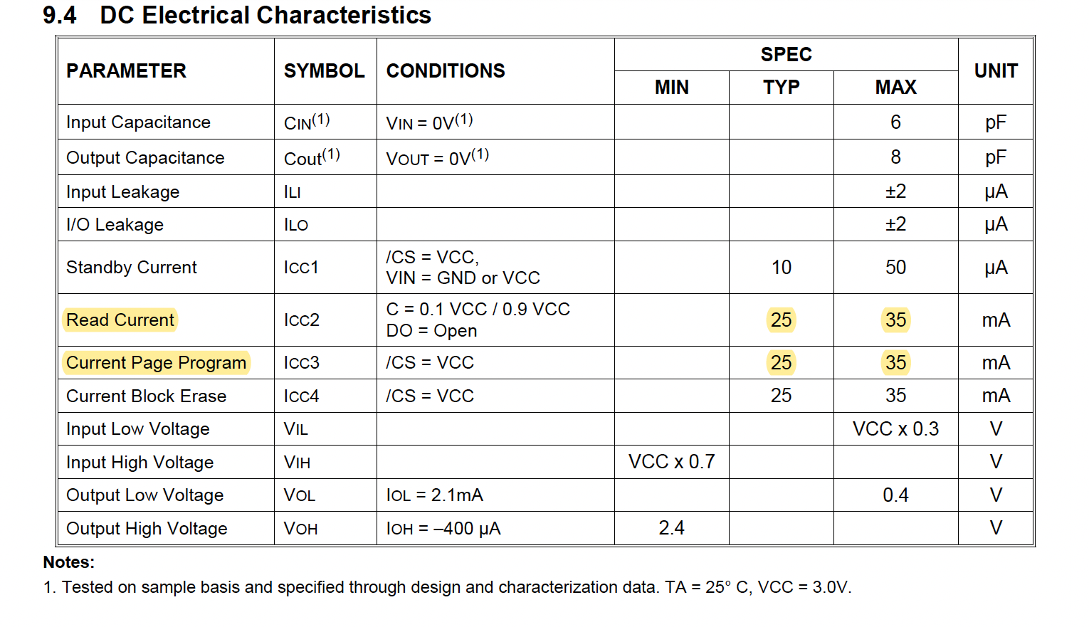
Typical and maximum power consumption of most components can be found by going through the Electrical Characteristics of each component in their respective datasheets. For example, the datasheet of on-board QSPI Flash shows that it typically consumes 25mA for Read/Page Program operations but could consume a maximum of up to 35mA as shown in the figure below.
The typical and maximum power consumption of secondary components on the OSDZU3-REF have been found and listed in the below tables. The components are separated into different tables based on the primary power rail they use. Components that use more than one power rail for their operation appear in multiple tables, for example U8 and U15. Components that consume negligible power, anything under 50mW, have been intentionally omitted from the power budget.
| Board Designator | PART # | Power Rail | RAIL Voltage | Typical Current (mA) | Maximum Current (mA) |
|---|---|---|---|---|---|
| U31 | MAX8902BATA+T | VIN_5V0 | 5 | 500 | 500 |
| J12 | USB3 Connector | VIN_5V0 | 5 | 500 | 900 |
| Total | 1000 | 1400 | |||
| Total Power | 5W | 7W | |||
| Board Designator | PART # | Power Rail | RAIL Voltage | Typical Current (mA) | Maximum Current (mA) |
|---|---|---|---|---|---|
| U8 | USB3320C-EZK-TR | PMIC2_C (3.3V) | 3.3 | 11.3 | 17 |
| U15 | 5P49V5935B536LTGI | PMIC2_C (3.3V) | 3.3 | 30 | 34 |
| U23 | EMMC04G-S100-B08U | PMIC2_C (3.3V) | 3.3 | 240 | 340 |
| U4 | AR8035-AL1A | PMIC2_C (3.3V) | 3.3 | 33.9 | 128 |
| J1 | SD CARD | PMIC2_C (3.3V) | 3.3 | 80 | 200 |
| U30 | FIN1019MTCX | PMIC2_C (3.3V) | 3.3 | 7 | 12.5 |
| U2 | W25N01GVZEIG_TR | PMIC2_C (3.3V) | 3.3 | 25 | 35 |
| U17 | 210-251P-BOARD | PMIC2_C (3.3V) | 3.3 | 20 | 70 |
| Total | 447.2 | 836.5 | |||
| PMIC2_C (3.3V) Maximum Allowed Current* | 1000 | 1000 | |||
| Current Headroom | 552.8 | 163.5 | |||
| Total Power | 1.48W | 2.76W | |||
| Board Designator | PART # | Power Rail | RAIL Voltage | Typical Current (mA) | Maximum Current (mA) |
|---|---|---|---|---|---|
| U8 | USB3320C-EZK-TR | VCC_PSAUX (1.8V) | 1.8 | 22.5 | 29.4 |
| U15 | 5P49V5935B536LTGI | VCC_PSAUX (1.8V) | 1.8 | 16 | 19 |
| Total | 38.5 | 48.4 | |||
| VCC_PSAUX (1.8V) Maximum Allowed Current* | 1000 | 1000 | |||
| Headroom | 961.5 | 951.6 | |||
| Total Power | 0.069 | 0.087 | |||
Step 2c: Combining Estimates of SiP and Secondary Components
Now that the typical and high use case power consumption estimates of OSDZU3 are available for PS, PL and on-board components, we can consolidate our estimates into one table and verify if currents on individual power rails and that our total power is within the allowed limits for the OSDZU3.
| OSDZU3 Allowed Limit | Typical Load | High Load | |||
|---|---|---|---|---|---|
| PL (Case 1) | PS (Case 3) | PL (Case 2) | PS (Case 4) | ||
| XCZU3 Input Power (W) | 15W (@5V) | 2.6W | 2.5W | 3.1W | 2.9W |
| LPDDR4 Input Power (W) | – | 0.19W | – | 0.49W | |
| OSDZU3 Internal Currents: | |||||
| VCCINT (A) | 3.75 | 2.7A | 0.33A | 3.26A | 0.34A |
| VCCAUX (A) | 1.0 | 0.16A | 0.38A | 0.17A | 0.4A |
| VCC_PSINTFP (A) | 1.5 | 0A | 1.05A | 0A | 1.3A |
| VCC_PSAUX (A) | 1.0 | 0.002A | 0.035A | 0.002A | 0.035A |
| OSDZU3-REF On-board Component Power (W) | 25W (U28: Main 5V Regulator Limit) | 6.55W | 9.85W | ||
| On-board Input Currents: | |||||
| VIN_5V0 (A) | 1A | 1.4A | |||
| PMIC2_C (A) | 1.0 | 0.447A | 0.837A | ||
| VCC_PSAUX (A) | 1.0 | 0.039A | 0.048A | ||
| Total OSDZU3-REF Input Power (W) | 25W (U28: Main 5V Regulator Limit) | Up to 9.24W (i.e., 2.5W + 0.19W + 6.55W) | Up to 13.24W (i.e., 2.9W + 0.49W + 9.85W) | ||
As seen in the above table, the currents on individual power rails and total power are within the allowed limits for the OSDZU3 SiP and OSDZU3-REF board.
Step 3 Extended: Estimating Losses
The various losses already described in the Estimating Losses section apply here as well on top of the following:
IR Losses
The traces used to supply power to the OSDZU3 will have a DC resistance, usually in the order of milliohms. IR loss is proportional to the board’s input power. DC resistance between external power supply and OSDZU3-REF’s input terminals:

The Power loss due to the trace resistance can be calculated using the following formula:

Step 4 Extended: Estimating Total Input Power for OSDZU3 Reference Design
To summarize, starting with the Power System Diagram and adding various losses discussed in the Estimating Losses section to the consolidated power numbers in Consolidation of Current and Power Figures table, we can estimate total input power of the design.
Calculating Worst Case Power of OSDZU3 SiP Considering Losses for Case 2:
XCZU3’s input power = 3.1W
LPDDR4’s input power = 0W
Other SiP components’ (internal EEPROM + QSPI) input power = 0.05W
Secondary components input power (from Table 13 and Table 14) = 2.76W + 0.087W = 2.847W
(Components on +VIN_5V0 rail ignored since this rail is not powered by IRPS5401 PMIC)
IRPS5401 PMIC’s input power considering 60% efficiency (worst case) =

=10W
Worst Case OSDZU3 Power for Case 2 = 10W (Worst Case)
Calculating Worst Case Input Power of entire OSDZU3-REF Reference Design Considering Losses for Case 2:
Step-down converter TPS56528DDAR (U28)’s loads are:
OSDZU3 SiP’s total Input Power (i.e., OSDZU3 + LPDDR4 + Other SiP components + Secondary Components powered by the SiP’s PMIC, all of which are calculated in previous step) + Secondary Components on +VIN_5V rail =
10W + 7W =
17W
TPS56528DDAR(U28)’s input power considering 92% efficiency (worst case)
=
= 18.48W
IR Loss (worst case): 10%
Worst Case OSDZU3 reference design power for Case 2:
=
=20.53W (Worst Case)
The OSDZU3-REF’s worst case power for all example use cases is calculated and shown in following table.
| OSDZU3 Reference Design Power Estimate – Worst Case | ||||
|---|---|---|---|---|
| Case 1 | Case 2 | Case 3 | Case 4 | |
| XCZU3 | 2.6W | 3.1W | 2.5W | 2.9W |
| LPDDR4 | – | – | 0.19W | 0.49W |
| Other SiP Components | 0.05W | 0.05W | 0.05W | 0.05W |
| On-Board Components on PMIC power rails | 2.85W | 2.85W | 2.85W | 2.85W |
| PMIC Load | 5.5W | 6W | 5.59 | 6.29 |
| PMIC Efficiency(worst case) | 60% | 60% | 60% | 60% |
| PMIC Input | 9.17W | 10W | 9.32W | 10.48W |
| OSDZU3 Input | 9.17W | 10W | 9.32W | 10.48W |
| On-Board Components on +VIN_5V0 rail | 7 | 7 | 7 | 7 |
| TPS56528DDAR’s Load | 16.17W | 17W | 16.32W | 17.48W |
| TPS56528DDAR efficiency | 92% | 92% | 92% | 92% |
| TPS56528DDAR’s input power | 17.58W | 18.48 | 17.74 | 19 |
| IR Loss % | 10% | 10% | 10% | 10% |
| OSDZU3 Reference Design Total Power (W) | 19.53 | 20.53 | 19.71 | 21.11 |
Revision History
Get notified of updates to this Application Note and all of our Technical Documentation.
"*" indicates required fields
| Revision Number | Revision Date | Changes | Author |
| 1 | 10/27/2023 | Initial Production Release | Eshtaartha Basu |
