OSDZU3 Layout Guide
Published On: September, 7, 2023 By: Eshtaartha Basu
The OSDZU3 was designed to minimize the number of Printed Circuit Board (PCB) layers and make the layout process easy. This document will cover important aspects of PCB layout design specific to the OSDZU3 and help designers quickly begin the PCB layout process. First, this document will discuss the layout of the OSDZU3 BGA. Then it will discuss a few common layout scenarios using relevant examples with recommendations on pours for Power, Ground, and other supporting circuitry.
This document assumes that the reader is already familiar with layout design process and the OSDZU3 Data Sheet. The document should not be used as a comprehensive layout tutorial or a generic layout design guide.

Table of Contents
OSDZU3 Layout Guide
The OSDZU3 System-In-Package (SiP) product consists of building blocks designed to allow easy and cost-effective implementation of systems based on AMD’s XCZU3 SoC. The OSDZU3 integrates the XCZU3 device along with two Infineon PMICs, two LDOs, LPDDR4 Memory, QSPI Flash Memory, an EEPROM for non-volatile configuration storage, resistors, capacitors, and inductors into a single 20.5mm x 40mm design-in-ready package.
This section will introduce important specifications, ball mapping and footprint information of the OSDZU3.
Background Information
AMD has a number of documents which will be useful to your design. One of those documents is the UltraScale Architecture PCB design guide (UG583). In that document there are 12 chapters. The following table lists the chapters separated into three categories. Those chapters of which 1) Octavo Systems followed while designing the OSDZU3, 2) the PCB designer should pay attention and 3) do not apply to the OSDZU3.
| Chapters of which Octavo referred to while designing the OSDZU3 SiP | |
|---|---|
| 1 | Power distribution System in UltraScale Devices. |
| 2 | PCB Guidelines for Memory Interfaces |
| Chapters of which the PCB designer should pay attention | |
| 1 | Power distribution System in UltraScale Devices |
| 4 | PCB Guidelines for the PS Interface in the Zynq UltraScale+MPSoC |
| 5 | PCB Routing Guidelines for MIPI D-PHY |
| 10 | Select I/O Signaling |
| 11 | PCB Technology Basics |
| 12 | Design of Transitions for High-Speed Signals |
| Chapters of which do not apply to a OSDZU3 SiP based design | |
| 3 | PCB Guidelines for Zynq UltraScale+RFSoCs. |
| 6 | Migration between UltraScale Devices and Packages |
| 7 | Migration between UltraScale and UltraScale+FPGAs |
| 8 | Migration between Zynq UltraScale+MPSocs and Packages |
| 9 | Migration between Virtex UltraScale+VU13P devices and VU27P/VU29P Devices |
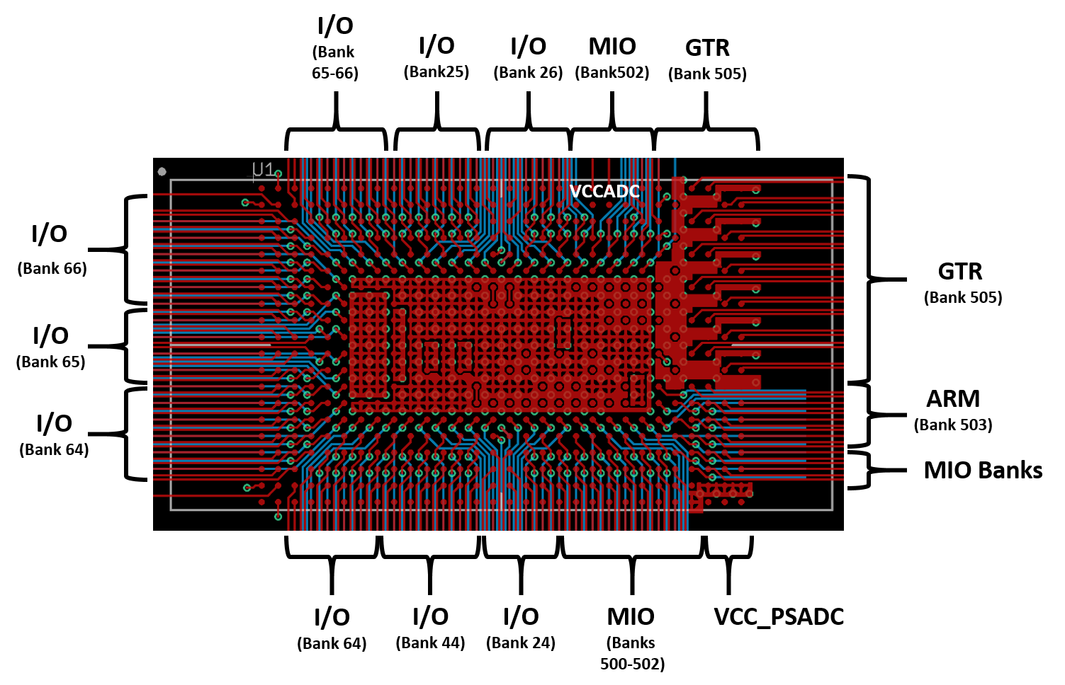
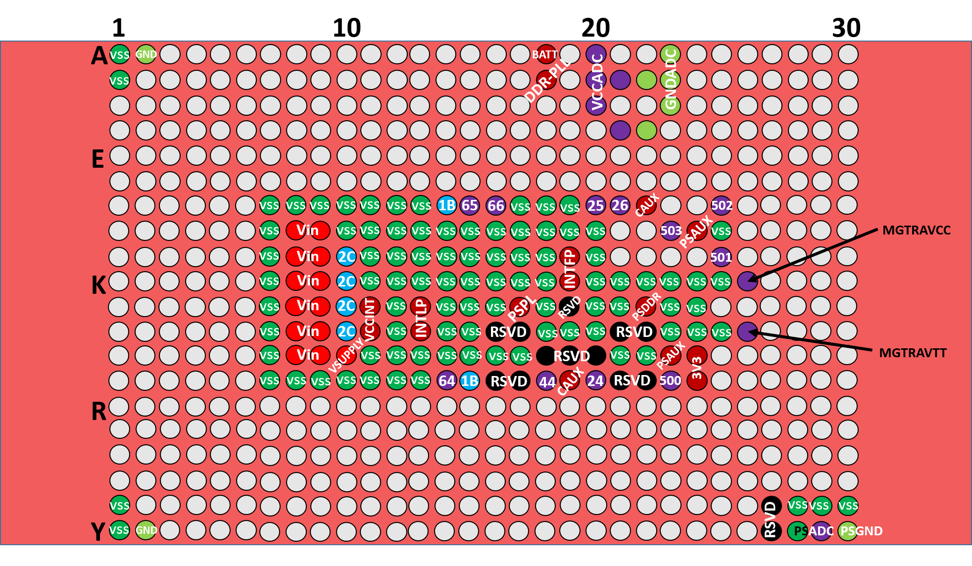
Ball Function Map
The Ball function map shown in the below figure provides a visual representation of the arrangement of the BGA balls of the OSDZU3. This can help with the placement and orientation of the OSDZU3 in a design. The ball map is shown from a top view looking through the package to the balls.
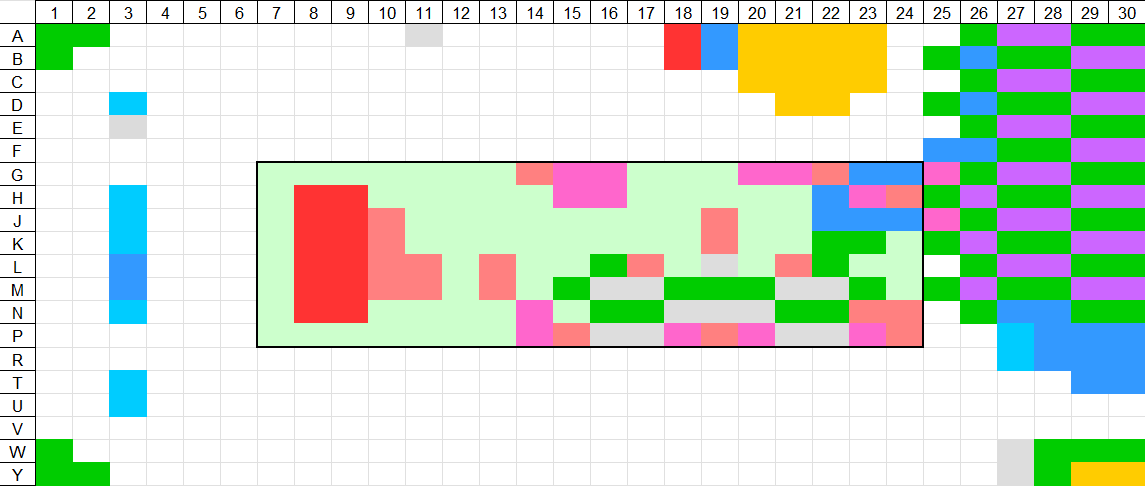
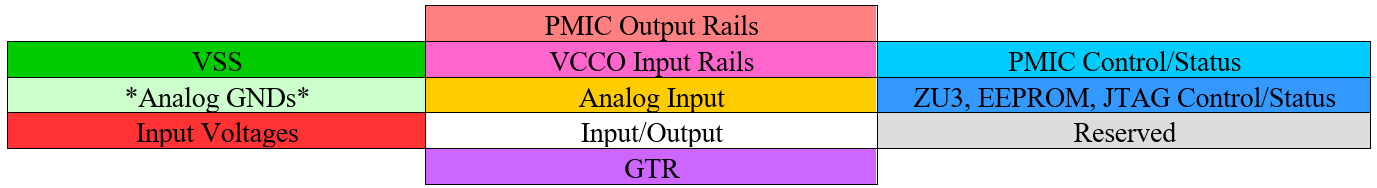
The ball map in the above figure is color coded to make it easier to use. Here is the color key for reading the ball map:
*GND_PSADC, GNDADC and GND_ANA are not connected to each other internally, nor are they connected to VSS.
Footprint Configuration
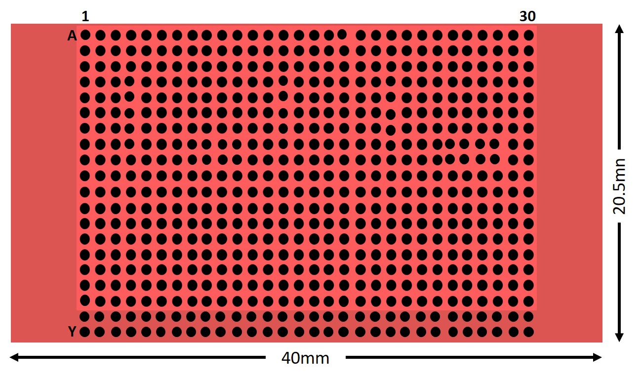
The OSDZU3 footprint parameters are shown in the 2 table below (Footprint Dimensions 1 and Footprint Dimensions 2); they are also listed in the table. Note the view is a top view.
| Parameter | Value |
|---|---|
| Package Dimension | 20.5mm x 40mm x 2.5mm |
| Number of Balls | 600 |
| Ball Grid | 20 rows x 30 columns |
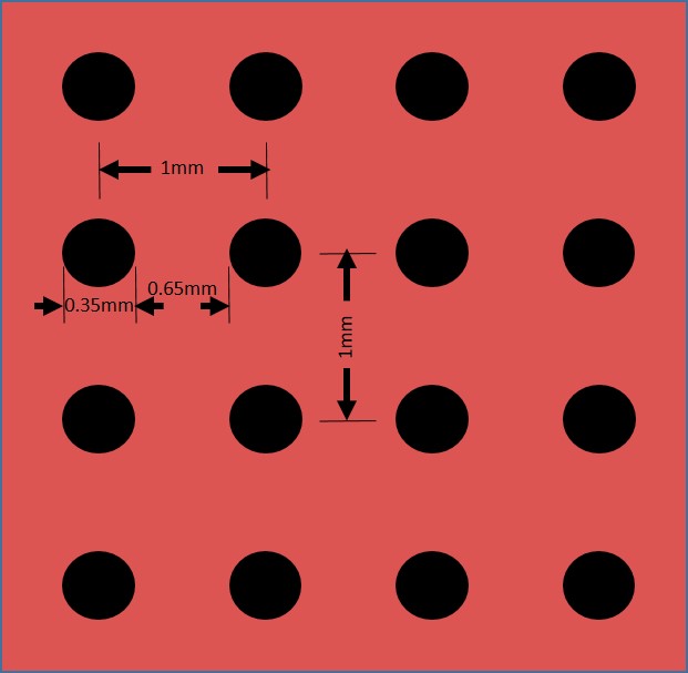
| Ball Pitch | 1mm (39.37mils) |
| Example Landing Pad Size | 0.35mm (13.78mils) |
The landing pad size was determined from the IPC-7351A specification. To find more information about landing pad sizes, refer Landing Pad Sizing section of OSDZU3 Datasheet.
For more information on the footprint configuration, please see the Mechanical Dimensions section of the OSDZU3 datasheet.
Routing and Vias
When pricing a PCB, the size of the traces and vias directly affect the cost to manufacture the board. Larger traces and vias, while cheaper, can make layout more difficult. Therefore, it is necessary to understand the optimum size of traces and vias for a given design. This section will provide background information on trace and via sizes and discuss layout tradeoffs when designing with the OSDZU3 BGA.
Trace Size Background Information
The number of traces that can pass between any two pads of a BGA footprint depends on the trace width and trace spacing. Trace width is the actual width of the trace. Trace spacing is the distance between the edges of any two adjacent traces or a trace and a pad. Trace width and trace spacing are shown pictorially in the figure.
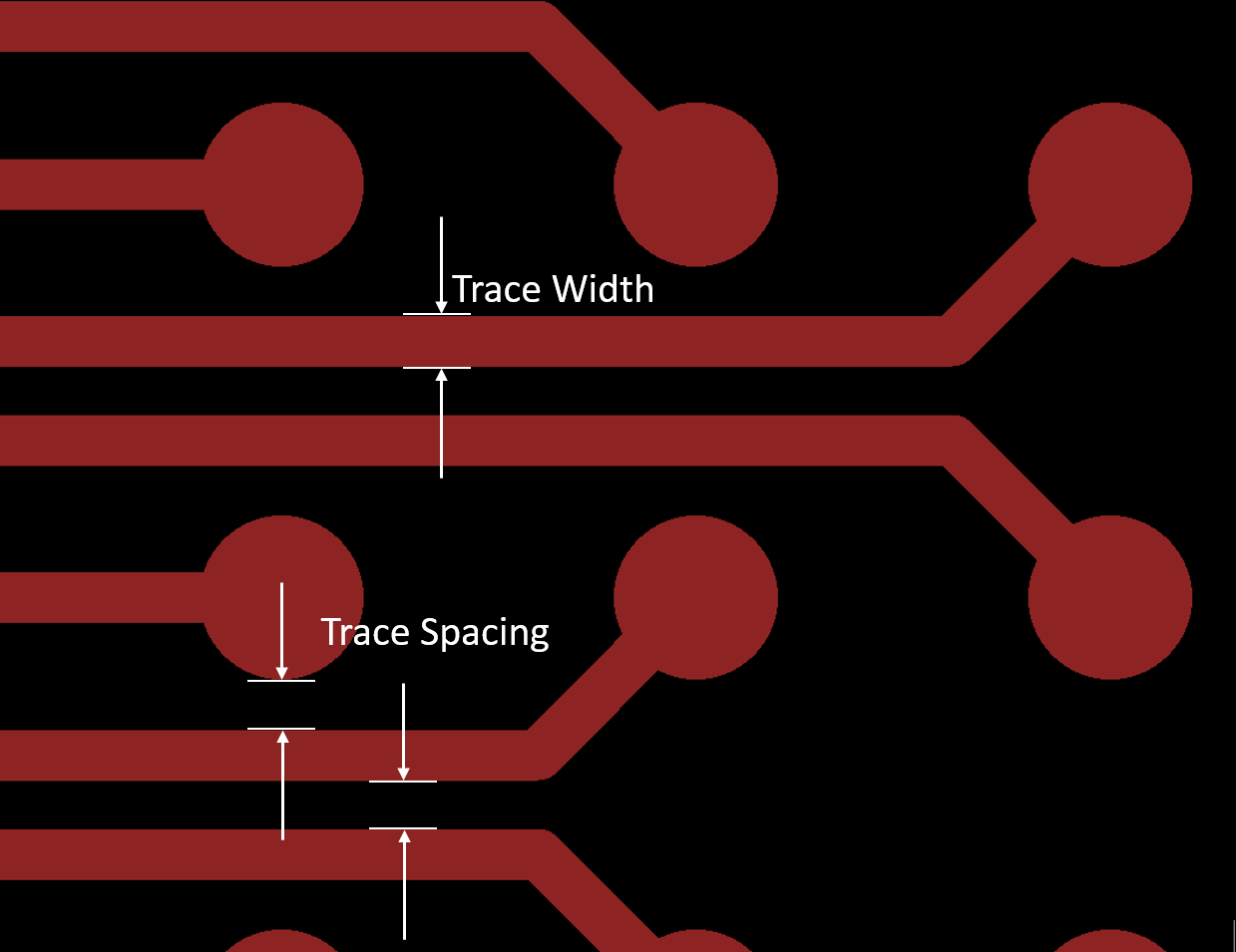
In this document, an “x/y trace” indicates a PCB that uses design rules with trace width of x mils and trace spacing of y mils. For example, a 5/6 trace indicates a PCB with trace width of 5mils and trace spacing of 6mils.
The number of traces that can be routed between any two adjacent pads of the BGA can be calculated using the formula (formula assumes all the traces are equal width):
tn tw + (tn + 1) ts <= BP – BD
where,
tn = number of traces
tw = trace width
ts = trace spacing
BP = BGA pitch
BD = BGA landing pad diameter
For example, to calculate the number of 5/5 traces that can be routed between adjacent pads of the OSDZU3 BGA: tw = 5mils, ts = 5mils, BP = 39.37mil (1mm) and BD = 13.78mil (0.35mm)
Using all this in the above equation:
5tn + 5(tn + 1) <= 25.59
10tn <= 20.59
tn <= 2.059 traces.
This result indicates that two (2) full 5/5 traces can be routed between adjacent balls of the OSDZU3 BGA. Similarly, the number of traces can be calculated for other routing rules.
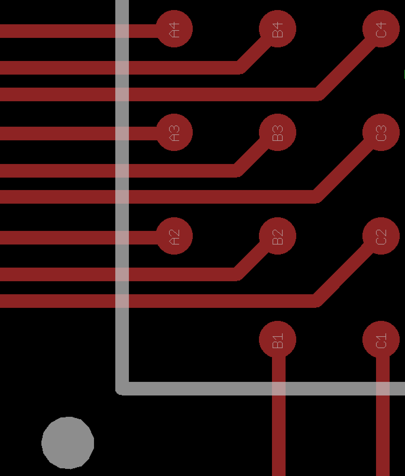
The below table lists examples of maximum equal trace and space widths for various numbers of traces between adjacent balls. In the OSDZU3 BGA, almost all the signal pins are in the first six rows / columns of the BGA. This means the signals can fully escape the BGA, by using 2 traces routed between each pair of balls on two interconnection layers of the PCB. See the OSDZU3 Layout Examples section for more details on how to handle the OSDZU3 signal fan-out.
| Maximum Equal trace and spacing width in mils (µm) | Number of traces between two adjacent BGA pads |
|---|---|
| 8.5/8.5 (215/215) | 1 |
| 5/5 (127/127) | 2 |
| 3.65/3.65 (92.5/92.5) | 3 |
| 2.84/2.84 (72/72) | 4 |
For the general case, if the trace and spaces are the same dimension, and the desired number of signal traces is n that can be placed between two balls, the required maximum trace, and spacing widths t(w),
in mils is:
t(w) = 25.59/(2n+1)
and in µm is:
t(w) = 650/(2n+1)
Example: 5/5 Traces Routed Between Pads of the OSDZU3
On all sides, the first three rows of OSDZU3 can be easily accessed using 5/5 traces as shown in following figure.
Via Size Background Information
There are two important parameters for vias: drill diameter and annular ring thickness. Drill diameter is the diameter of the drilled hole in the PCB. The annular ring thickness is the thickness of the pad that surrounds the drilled hole. These dimensions are shown in the figure.
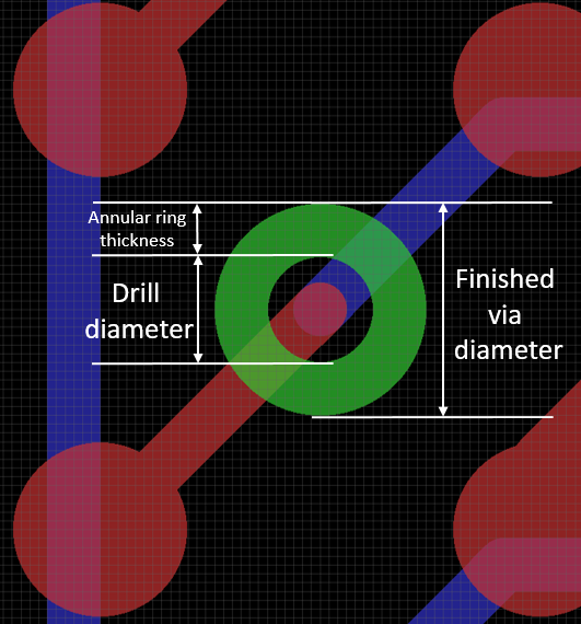
To determine the diameter of the finished via, use the following formula:
Finished via diameter = Drill diameter + 2 x (Annular ring thickness)
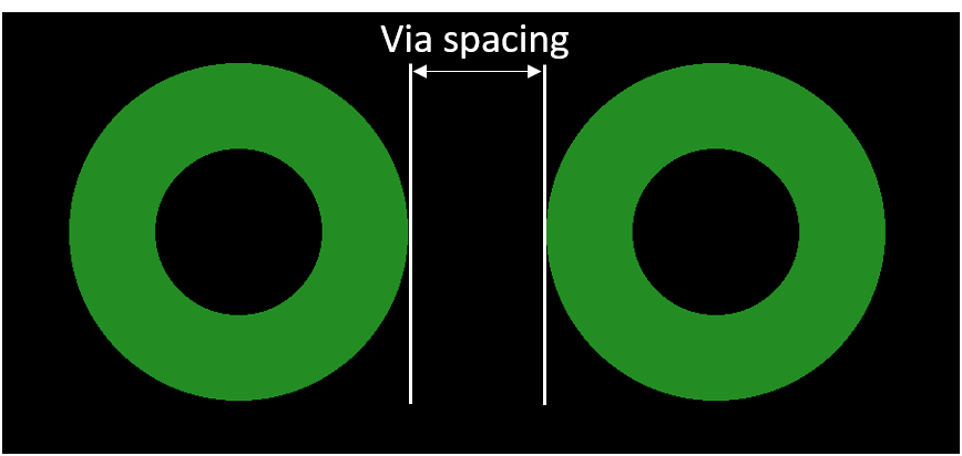
Via spacing is the distance between the edges of any two adjacent vias as shown in the below figure. When placing vias, make sure the spacing between the vias matches the trace spacing design rules that were chosen.
In this document, a “x/y via” indicates a via with drill diameter of x mils and finished via diameter of y mils. For example, a 12/24 via indicates a via with drill diameter of 12mils and finished via diameter of 24mils.
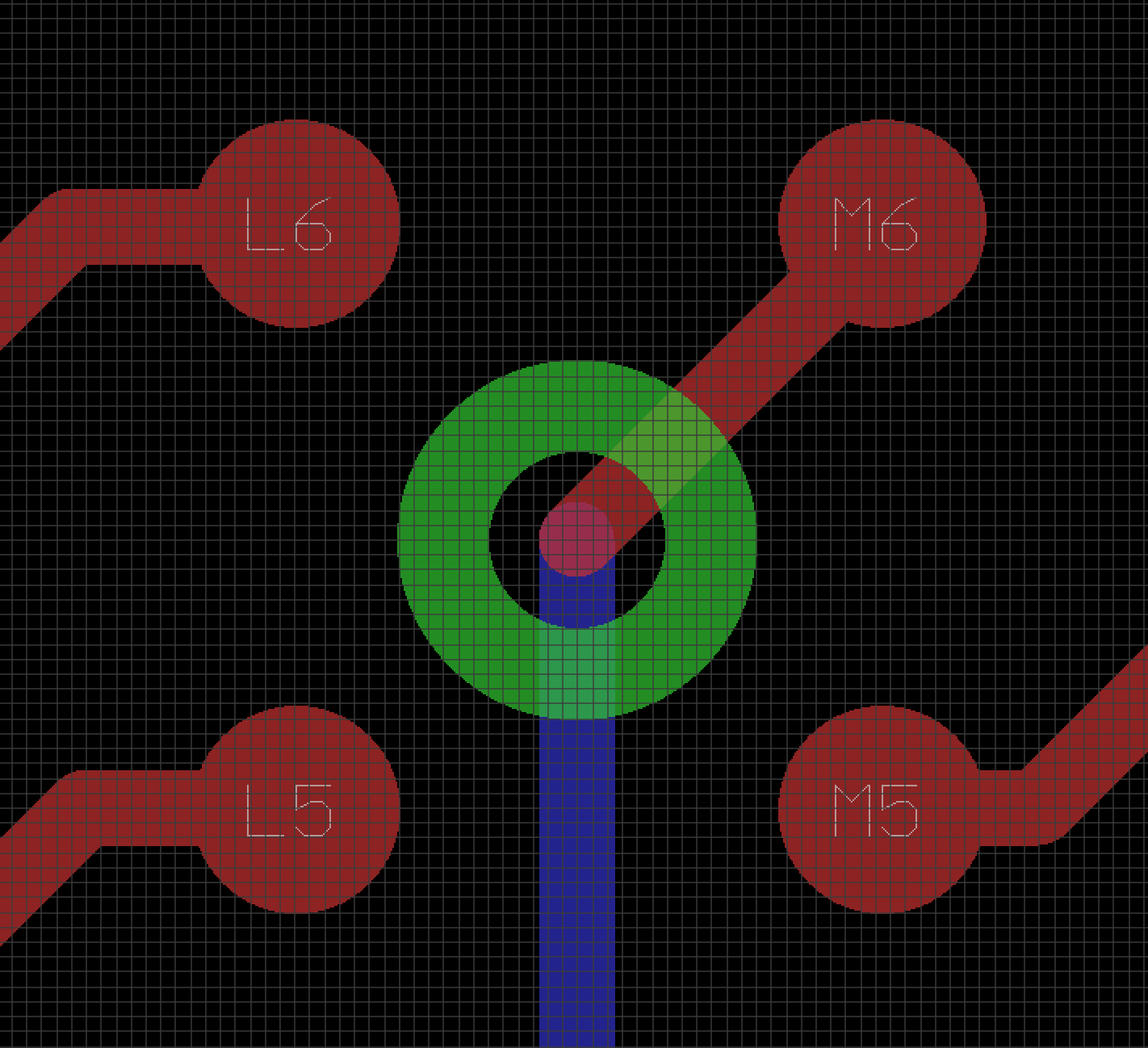
Example: A 12/24 Via Between 4 Pads of the OSDZU3
One 12/24 via can be easily placed between four adjacent balls of the BGA as shown in the below figure. A 12/24 via falls under the Standard Manufacturing capabilities of most PCB manufacturers.
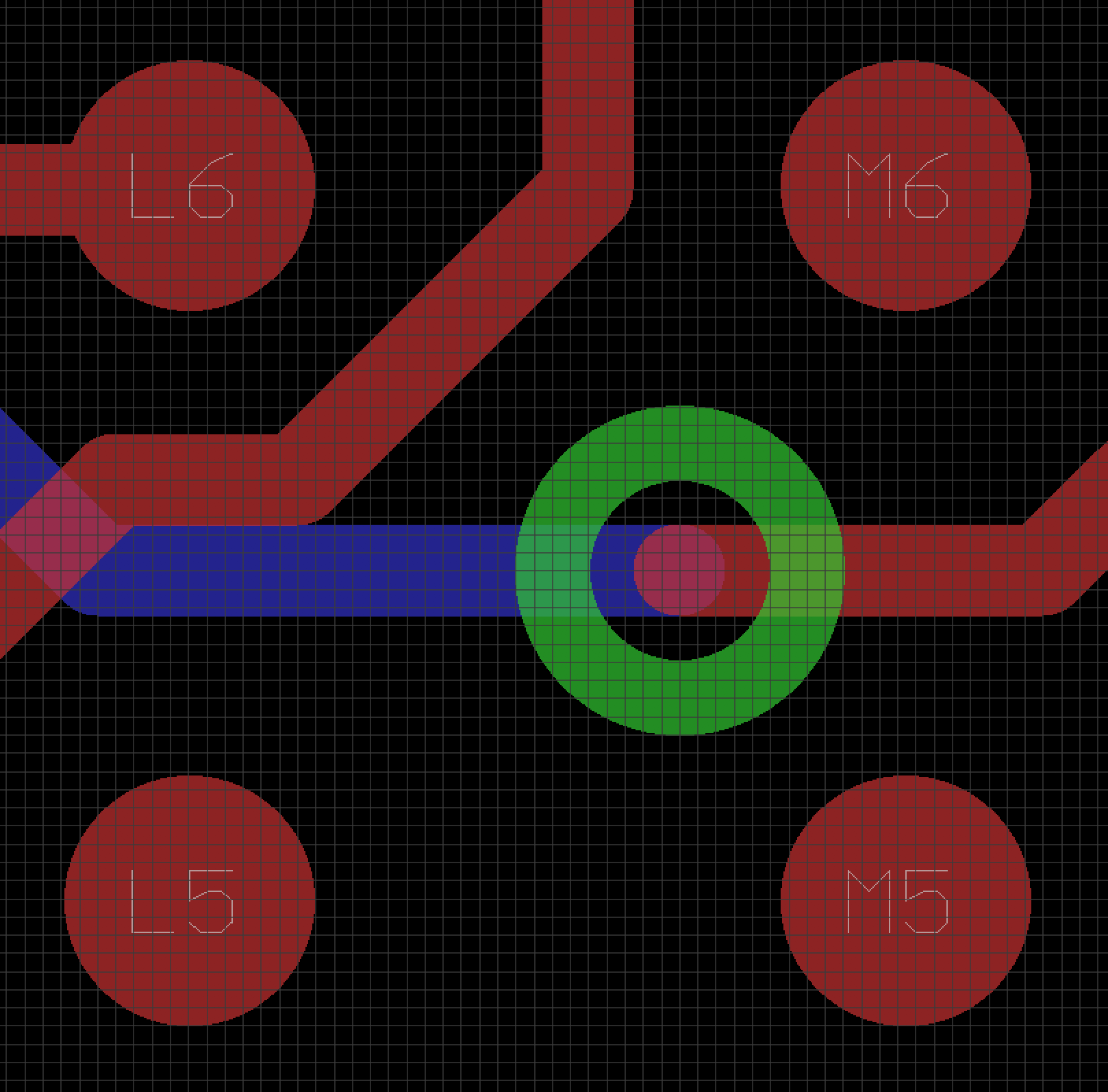
Example: A 10/18 Via and 5/5 Trace Between 4 Pads of the OSDZU3
The figure shows one 10/18 via and one 5/5 trace between four adjacent pads of OSDZU3.
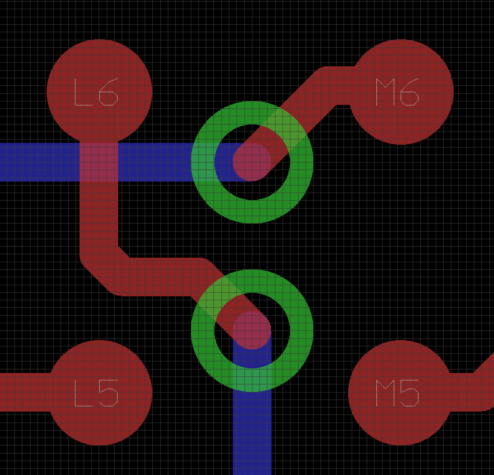
Example: Two 10/16 Vias Between 4 Pads of the OSDZU3
In case of a tighter design, two 10/16 vias can be placed between four adjacent balls of the BGA as shown in Figure 10. A 10/16 via falls under Extended Manufacturing capabilities of most PCB manufacturers. This via size may be slightly more expensive than 12/24 via. However, based on your manufacturer’s capabilities and your design requirements, you could choose to use a much smaller via than 10/16.
OSDZU3 Layout Examples
Once the design rules for traces and vias have been chosen for the PCB, the BGA can be routed. The following sections provide examples of how to lay out the PCB with an OSDZU3 SiP. Because the integration inside OSDZU3 SiP, it is possible to reduce the number of PCB layers needed for the design to 4 or 6 layers.
Signal Pin Fanout
The following figure shows the fanout of all pads of the OSDZU3 using 5/5 traces and two layers of the PCB.
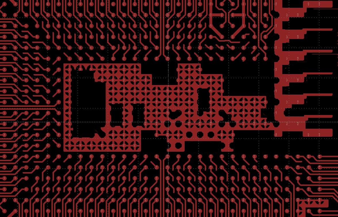
Power Inputs and Outputs
Power to the two input power rails (+5V_VIN and VCC_PSBATT) of the OSDZU3 can be supplied through a copper pour and vias as shown in Figure 13. Also, power from the output power rails of the OSDZU3 can be connected to the PCB using copper pours as shown in Figure 13.
Ground Connections
The ground pins of the OSDZU3 can be connected to ground plane using copper pours as shown in the figure.
It is recommended that you have as many vias as possible in the GND pour to aid heat dissipation.
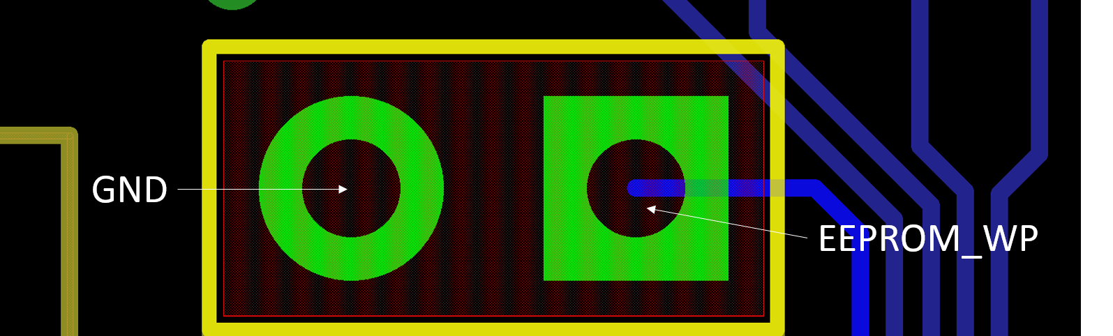
EEPROM
The write protect pin of the EEPROM (EEPROM_WP) of the OSDZU3 needs to be driven low before information can be written into it. This can be done in many ways: The EEPROM_WP pin can be driven by another device on the PCB; It can be driven by one of the OSDZU3 pins; It can be routed to a pad to be driven by an external device; It can be routed to a jumper; etc.
The below figure shows an example of the EEPROM_WP pin routed to a jumper using 100mil header. The other side of the jumper is connected to GND which allows the EEPROM_WP signal to be easily driven low. This can be a useful layout in prototype designs that are not space constrained.
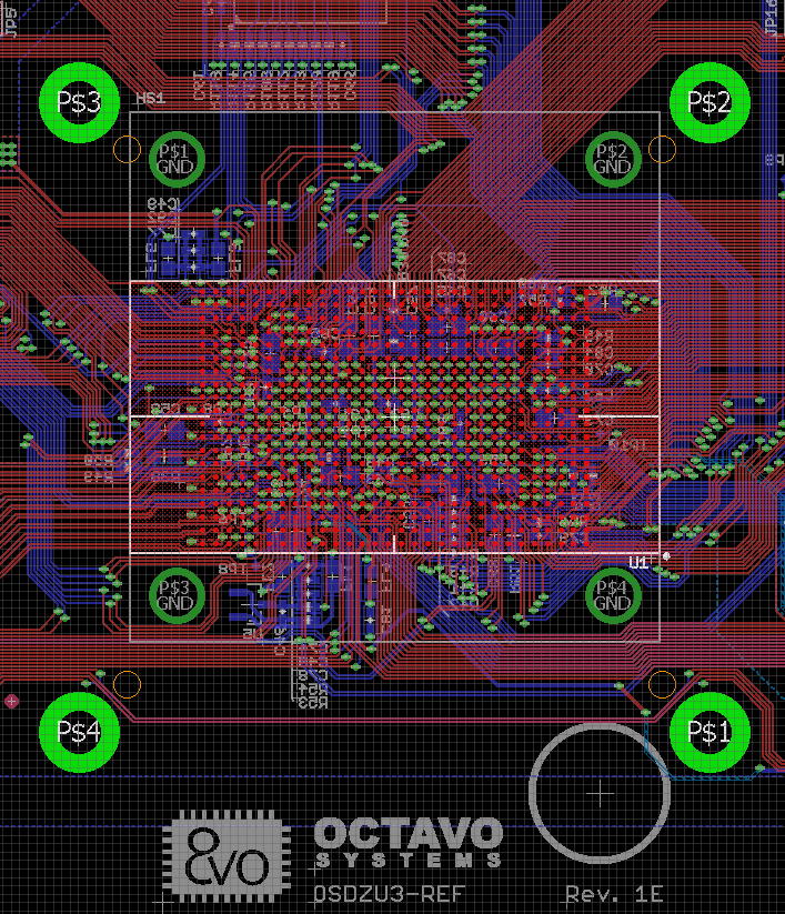
Thermal Considerations
In a BGA package, typically 80-90% of the heat is dissipated via BGA balls to PCB. However, some applications or board designs may make it necessary to use a heat sink. In such cases a provision should be made in the PCB design to fasten the heatsink to OSDZU3 as well as to the PCB. As an example, the heatsink holes provisioned in the OSDZU3-REF PCB layout design is shown below. For more detailed information on heatsink recommendation and thermal parameters for the OSDZU3 SiP, please refer the OSDZU3 Thermal Guide.

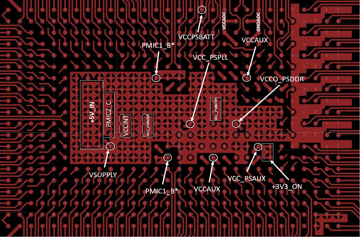
External Capacitor Placement
It is recommended that the external bulk capacitors be placed as near to the appropriate power balls of the OSDZU3 SiP as possible. The figure below shows the location of the balls for the various OSDZU3 voltage rails.
Note: The bulk capacitors may be placed on either side of the PBC.
If space is available, it is recommended that additional capacitor footprints be added to the PCB design which will accept a variety of bulk capacitor values. Capacitors can be inserted when needed or the footprints left unpopulated (DNI). If it becomes necessary to place the capacitors away from the OSDZU3 footprint due to space constraints, try to use at least 15mil traces between the capacitors and corresponding BGA balls.
For more information on capacitor placement, please refer the following recommendations from AMD:
- https://docs.xilinx.com/r/en-US/ug583-ultrascale-pcb-design/Capacitor-Placement-Background
- https://support.xilinx.com/s/question/0D52E00006jqrT6SAI/zynq-ultrascale-decoupling-capacitance-and-power-rail-bulk-capacitance?language=en_US
References
Revision History
Stay up to date on changes to this app note and other information from Octavo Systems by signing up for our newsletter.
"*" indicates required fields
| Revision Number | Revision Date | Changes | Author |
| 1 | 09/07/2023 | Production Release | Eshtaartha Basu |
