OSDZU3 Vivado Tutorial
Published On: January, 16, 2023 By: Eshtaartha Basu | Updated: December 5, 2023 by Greg Sheridan
This tutorial will walk you through generating a hardware platform in Vivado 2021.2 for a design using the OSDZU3 System-in-Package. It will use the OSDZU3-REF platform as an example.
Here is a video walking through this app note you can watch and follow along with as well!
Objectives
At the end of this tutorial, you will be able to:
- Install the Board Definition Files for the OSDZU3 SiP and OSDZU3-REF platform in Vivado 2021.2
- Build a hardware platform in Vivado 2021.2 for a OSDZU3 based board (OSDZU3-REF)
- Create custom GPIO IP configuration
- Add custom GPIO Constraints
- Export the hardware platform as .xsa file (for use with Vitis 2021.2 if necessary)
Table of Contents
Tutorial Requirements
This tutorial will require the following software and hardware setups.
Software
The software requirements for this tutorial are:
- Xilinx Vivado v2021.2 (Xilinx account and licenses may be required)
- When running the installer, ensure the Install Cable Drivers option is enabled.
- Ensure this Xilinx patch is applied to your Vivado installation before proceeding further with this app note: https://support.xilinx.com/s/article/76960?language=en_US
- The appropriate OSDZU3 Board Definition Files provided by Octavo Systems and DesignLinx Hardware Solutions.
- OSDZU3-REF Board Definition – Files provided by Octavo Systems and DesignLinx Hardware Solutions, Linked Below.
- osdzu3_helper.tcl file below provided by Octavo Systems and DesignLinx Hardware Solutions, Linked Below. Putty terminal program
Hardware
The hardware setup for this tutorial is:
- PC with 4 GB RAM and 1 GB virtual memory (recommended)
- OSDZU3-REF platform
- 12V power supply (provided with OSDZU3-REF board)
- USB A-micro-B cables (2)
Installing the OSDZU3 and OSDZU3-REF Board Definition Files
The following Board Definition Files are provided to suit your needs and help with the hardware platform generation:
- OSDZU3EG1-2G 3V3 SiP
- Choose this BDF file for devices with a 3.3V QSPI and that require bank 500 IO to be 3.3V
- OSDZU3EG1-2G 1V8 SiP
- Choose this BDF file for devices with a 1.8V QSPI and that require bank 500 IO to be 1.8V
- OSDZU3 Reference Design
- Choose this BDF file for OSDZU3 Reference Design that uses a OSDZU3 SiP with a 3.3V QSPI and requires bank 500 IO to be 3.3V
The Board Definition Files must be installed in Vivado by either of the two methods below.
Method 1
Unzip the osdzu3_bdf.zip to the following folder of the Vivado 2021.2 install directory
<install_location>\Vivado\2021.2\data\xhub\boards\XilinxBoardStore\boards\Xilinx\
Method 2
Add a path to Vivado for a separate Board Repository
- Unzip the given osdzu3_bdf.zip to a folder that will contain the Board Repository
- Launch Vivado 2021.2
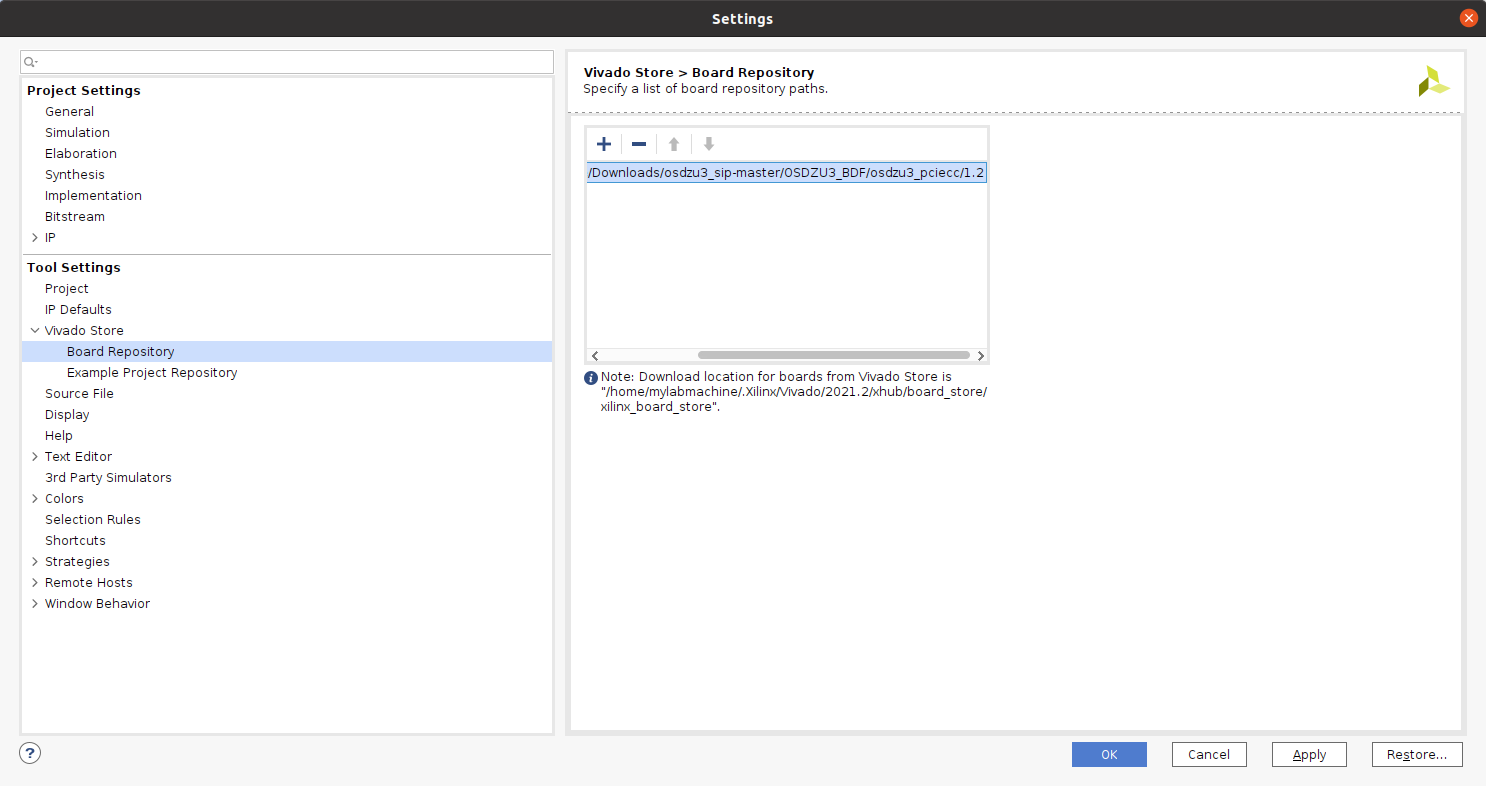
- Select Tools -> Settings
- In the Settings window, open the Vivado Store tab under Tool Settings.
- Select the Board Repository tab.
- Add the path to the Board Repository.

Add Path Dialog
Creating a Hardware Platform for the OSDZU3-REF board
This section will show you how to start with one of the OSDZU3 based Board Definition Files (BDFs), create a hardware platform, generate corresponding bit stream, and export the hardware platform as necessary.
We will be using OSDZU3-REF as our example platform. The on-board User Push Buttons, LEDs and DIP Switches will be exercised to illustrate the hardware platform generation process.

If you’re planning to use OSDZU3 Reference Design BDF for this process, skip sections 5.3.2, 5.3.3 and 5.6, follow all other steps below. This is because the skipped sections talk about manual GPIO IP configuration and adding GPIO constraints. These are not required for OSDZU3 Reference Design BDF since GPIO IP configuration and constraints for all on-board peripherals are already defined in the BDF.
Creating Vivado Hardware Platform Project
Please follow the steps shown below to create a hardware platform project.
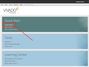
- Start the Vivado tool via Start > All Programs > Xilinx Design Tools > 2021.2 > Vivado 2021.2
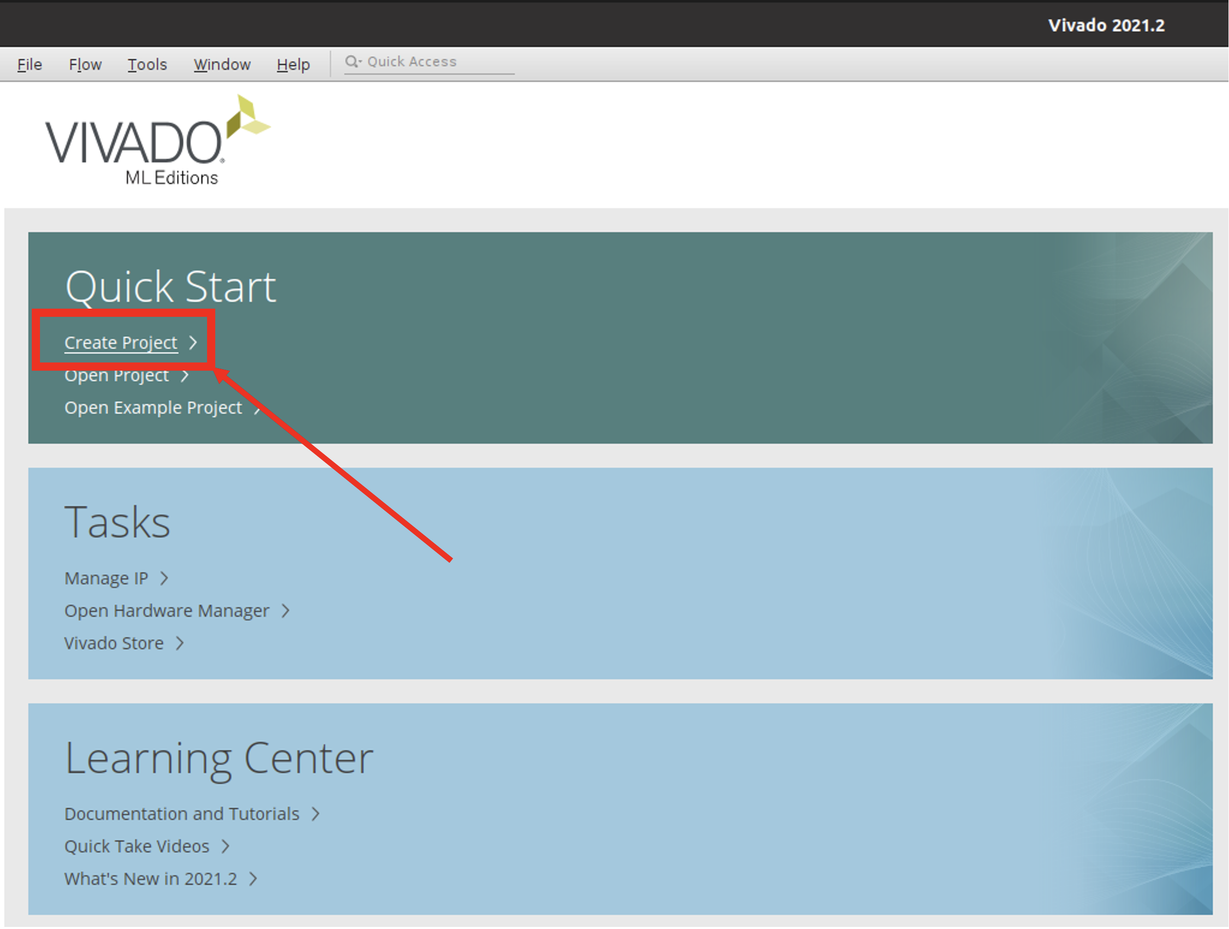
- Select Create Project.

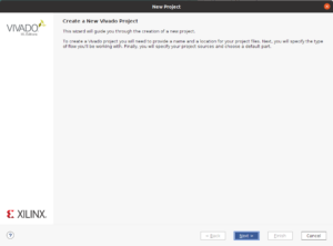
Create Project - Click Next to continue.

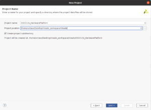
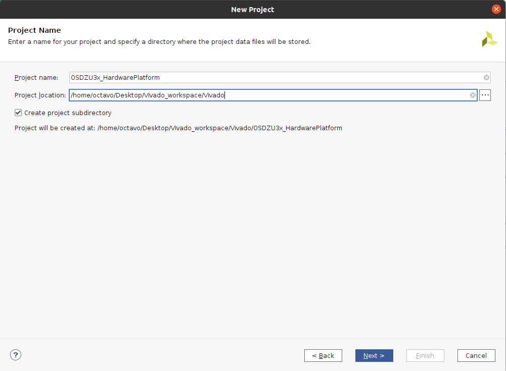
New Project Dialog - Set the project name and location and click Next to continue. Make sure the Create project subdirectory box is checked as shown in the following figure.

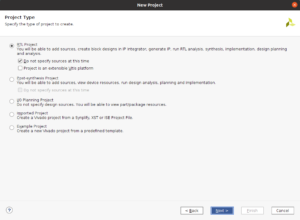
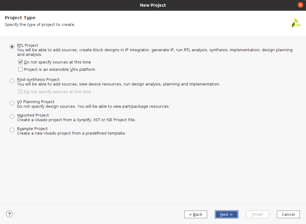
Enter Project Name - Select the RTL Project type and make sure the Do not specify sources at this time box is checked as shown in the following figure. Click Next to continue.
RTL Project Selection - In the Default Part dialog box
- Search for OSDZU3 under Boards
- Select one of the three BDFs, as per your requirement:
- Click Next
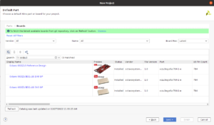

New Project Default Part Selection - In the New Project Summary dialog box, click Finish to continue.
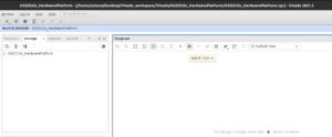
- Ensure your Vivado Project Summary indicates your required Board Part and other settings.

Creating a Block Design
In this section we will be creating a Block Design for the hardware platform. Once the Block Design canvas is created, IP cores can be added to the design from the Vivado IP Catalog.
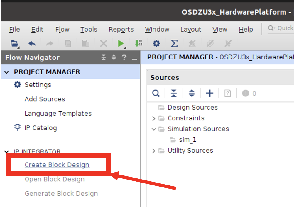
- Click on the Create Block Design as shown in the following figure.


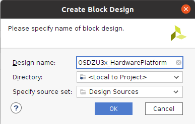
Create Block Design - When the following dialog box appears, click OK to continue. You may change the default design_1 name to anything you wish. We will be using the name shown in below figure for this tutorial.


Create Block Design Dialog - Click on the Add IP (+) icon in the white canvas area as shown in the following figure to begin adding IP cores to the design.

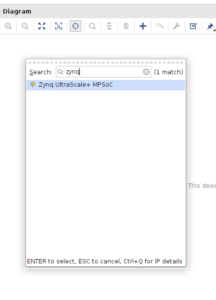
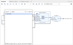
Block Designer Canvas - The first step is to add the Zynq IP core to the design. Type Zynq in the Search box and then double-click on the ZYNQ UltraScale+ MPSoC.

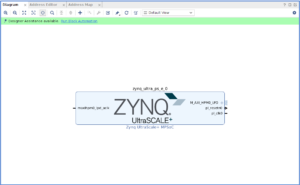
Adding IP Core - Zynq IP will be added to the design as shown in the following figure.

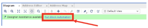
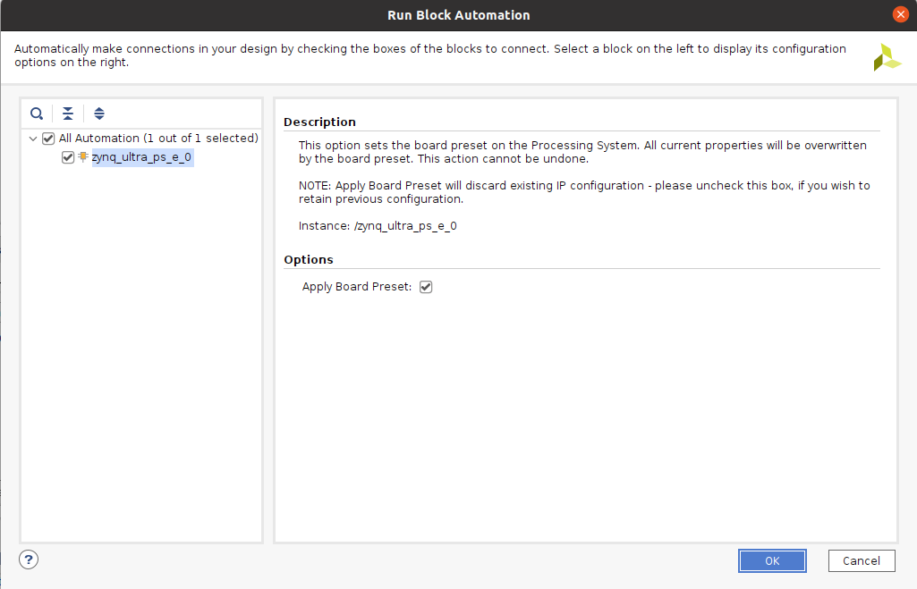
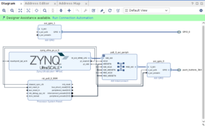
Zynq IP Core Added to Canvas - The Zynq device has not yet been configured for the chosen BDF. Click on the Run Block Automation to configure the Zynq device with the BDF settings.

Run Block Automation - When the following dialog box appears, click OK to continue.
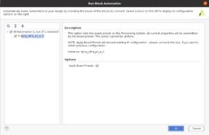

Select OK in the Run Block Automation Dialog - The Zynq device is now configured with the chosen BDF board level settings such as PS LPDDR4, PS peripheral selections, clocking, IO pin mapping etc.


Adding Peripherals to the Block Design
You are now ready to add peripherals to the design that are connected to the Zynq UltraScale+ MPSoC PL such as PL LEDs, DIP switches and Push buttons.
Adding Push buttons (using GPIO IP configuration and Constraints from Board Definition File)
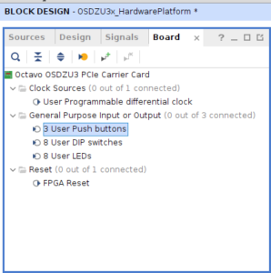
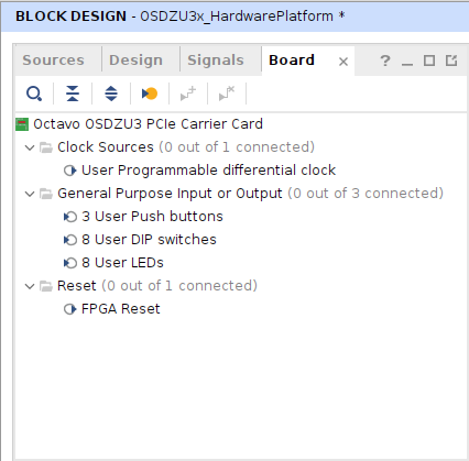
- Under Block Design window in Vivado, click on the Board tab as shown in the following figure. You will see a set of peripherals that can be connected to the Zynq UltraScale+ MPSoC PL on the OSDZU3-REF board under General Purpose Input or Output.
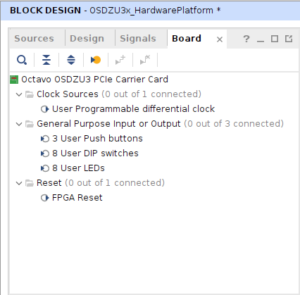

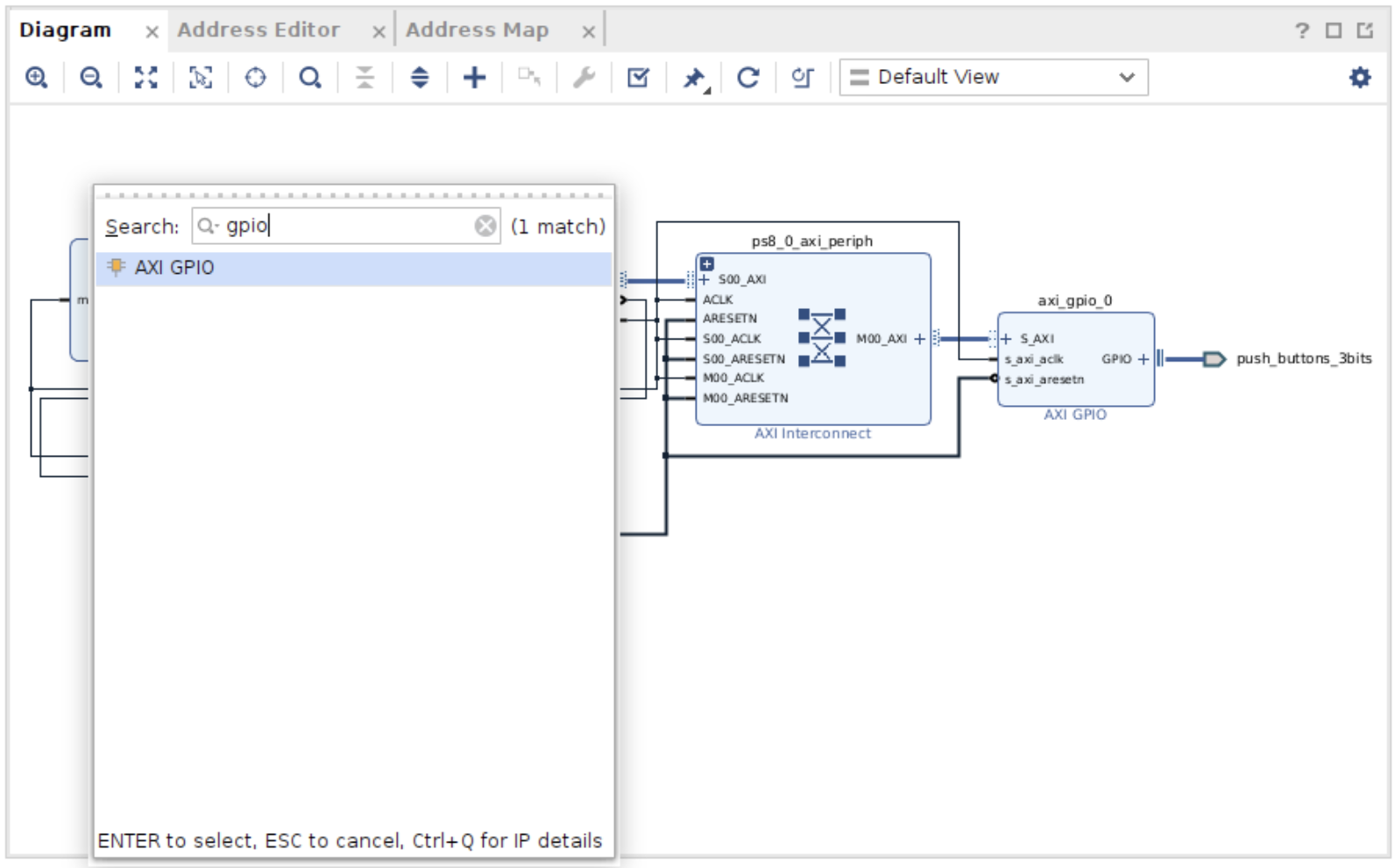
Boards Tab - Double click on the Push buttons as shown in the following figure to add the external PL Push switches to the design. This will add a PL GPIO core to the design so that the Push switches can be read via the Zynq UltraScale+ MPSoC PS.

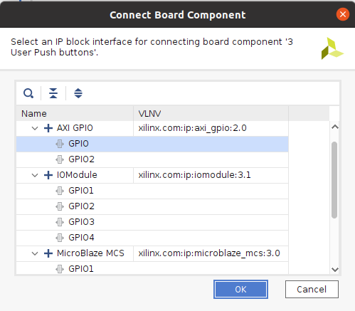
Push Buttons Selected - When the following dialog box appears, select the GPIO under the Create new IP as shown and then click OK.


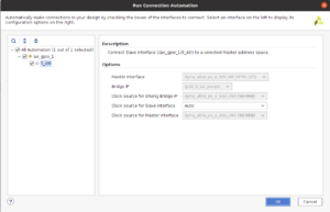
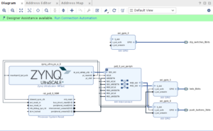
GPIO Selected under Create New IP - Click on the Run Connection Automation to connect the axi_gpio_0 IP (the new GPIO just added to the design) to the Zynq UltraScale+ MPSoC PS as shown in the following figure.
- When the following dialog box appears, click OK to continue.
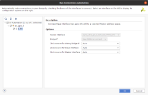
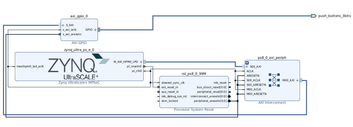
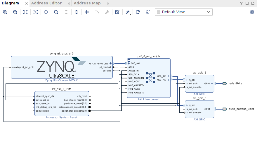
Run Connection Automation Dialog - The block design will look as shown in the following figure.
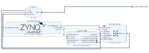

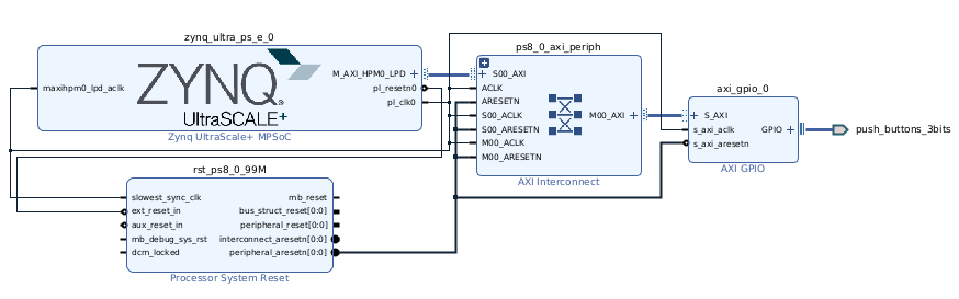
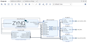
Block Design after Generation - Right-click in the white space of the block design diagram and select Regenerate Layout. This will clean up the block design drawing and places all PL peripheral interfaces to the right of the block design.
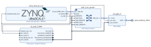

Block Diagram after Regenerate Layout - Skip to Validating the Block Design section because the next two sub-sections talk about manual GPIO IP configuration. This is not required for OSDZU3 Reference Design BDF since GPIO configuration for all on-board peripherals is already defined in the BDF. If you want to add LEDs/DIP Switches to your Block Design, the process is same as that of Push Buttons.


Adding LEDs (custom GPIO IP configuration)
To add LEDs with manual GPIO IP configuration:
- Select the + icon to add a new IP core to the design.
- In the search field, type GPIO
- Double click on the AXI GPIO to add it to the canvas.

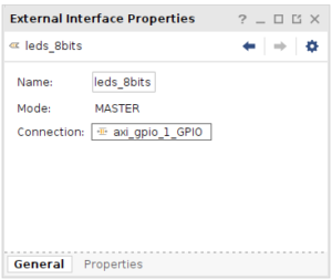
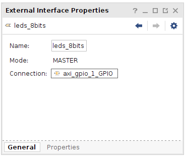
Adding AXI GPIO - In the canvas, select the output port of the GPIO port on the newly added GPIO IP core. Right-click and select Make External. This will add an output port to the design that is connected to the GPIO IP core.

GPIO Core set to External - Select the newly create external output port GPIO_0. In the Name field of the External Interface Properties window, replace the current name of GPIO_0 with the leds_8bits
 Renamed GPIO port
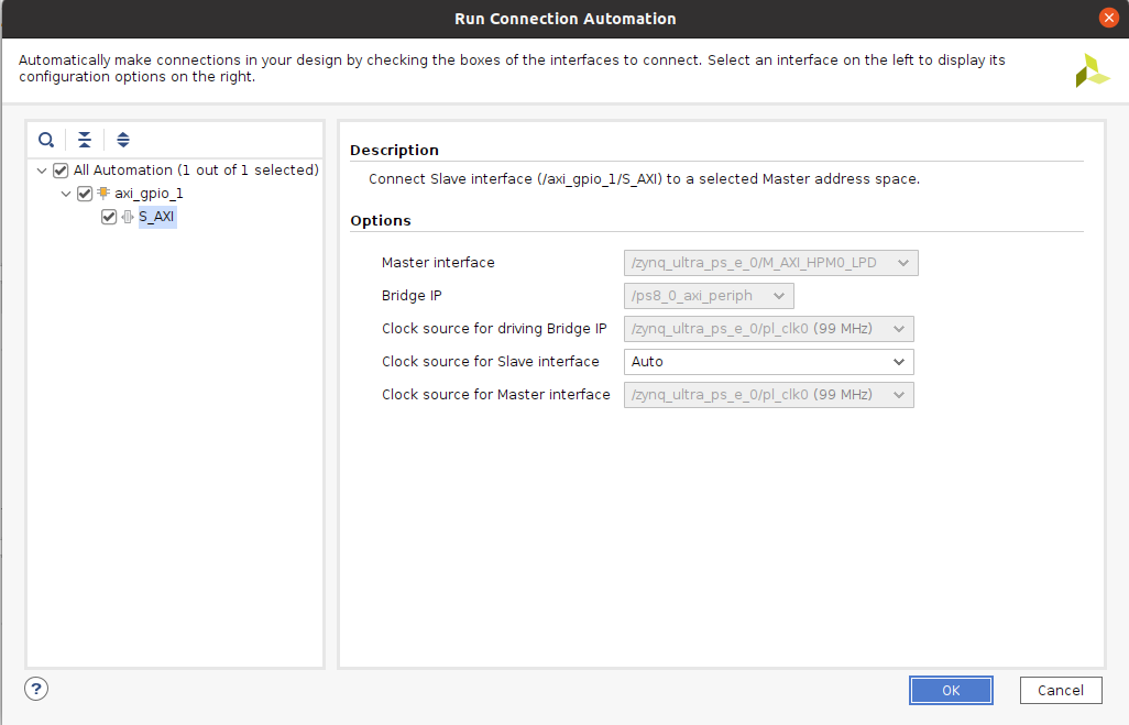
- In the canvas, select the Run Connection Automation link to properly connect the new GPIO to the system. Click OK in the window below.
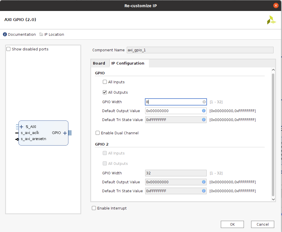
Run Connection Automation - Double-click on the LED GPIO IP (axi_gpio_1) to open the Parameterization GUI. Select the IP Configuration tab. Select the All Outputs check box. Set the GPIO Width to a value of 8. Select OK.


GPIO IP Configuration Tab - Right-click in the white space of the block design diagram and select Regenerate Layout.


Regenerated Layout

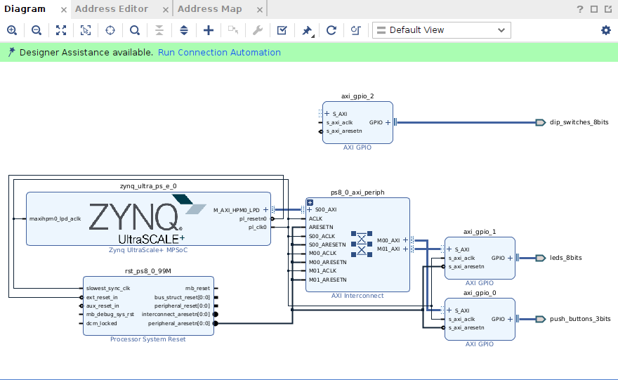
Adding DIP switches (custom GPIO IP configuration)
The process of adding DIP switches to the block diagram is similar to that of adding LEDs in the previous section.
- Add another AXI GPIO IP core.
- Make the output of the GPIO IP core external and rename it to dip_switches_8bits
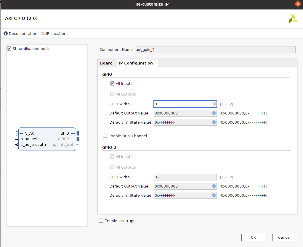
GPIO Dip Switches being added to design. - Set the configuration of axi_gpio_2 as shown below.


AXI_GPIO_2 Configuration - Regenerate layout.
Regenerated Layout

Validating the Block Design
- Select Tools > Validate Design from the Vivado toolbar as shown in the following figure. This will validate the design to make sure all block design connections are valid.
- When the following dialog box appears, click OK to continue.
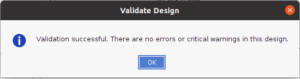

Successful Design Validation Dialog
Note: You may see 3 warning messages in the Vivado console. You can safely ignore these messages.
Creating HDL Wrapper File for the Design
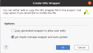
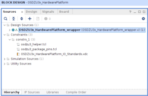
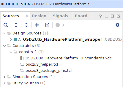
- Click on the Sources tab as shown in the following figure. Then right-click on the OSDZU3x_HardwarePlatform.bd and select Create HDL Wrapper. This will create a top-level HDL wrapper file for the design.
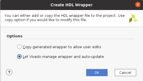
- When the following dialog box appears, click OK to continue.

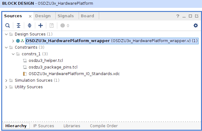
Create HDL Wrapper Dialog - The top-level Verilog wrapper file will be generated as shown in the following figure.

Project Explorer with HDL wrapper created
Adding Custom GPIO Constraints for the OSDZU3 SiP
Vivado (from AMD-Xilinx), by default, supports only Xilinx devices and their pin locations in the software. Since OSDZU3 SiP integrates Xilinx MPSOC within it, the pin locations between Xilinx MPSOC and the SiP may be different. As a result, the osdzu3_helper.tcl file is provided to aid in the translation from OSDZU3 pin locations to the pin locations of the surrogate Xilinx device that Vivado supports instead. The file also helps with timing calculations for IPs that have timing requirements.
- Create a new constraints file to hold the IO Standard constraints:
- In the Sources tab, select the + icon to open the Add Sources window.
- In the Add Sources window, select Add or create constraints, click Next.
- Select Create File and add the name of the new file (OSDZU3_HardwarePlatform_IO_Standards) to the File name: field. Click OK. Click Finish.
- In the Sources tab, double click on the new XDC constraints file to open it in the text editor.
- Cut and paste the following lines into the file:
# LED IO Standard set_property IOSTANDARD LVCMOS18 [get_ports {leds_8bits_tri_o[*]}] # DIP Switch IO Standard set_property IOSTANDARD LVCMOS18 [get_ports {dip_switches_8bits_tri_i[*]}] - Save the file.
- Create a new constraints file to hold the Pin Location constraints:
- In the same folder that now holds the new XDC constraints file, create a new file called osdzu3_package_pins.tcl.
- Open the new Tcl file in a text editor and cut and paste the following lines:
# LED pin location constraints tclapp::octavo::osdzu3::set_osdzu3_package_pin E7 [get_ports {leds_8bits_tri_o[0]}] tclapp::octavo::osdzu3::set_osdzu3_package_pin F7 [get_ports {leds_8bits_tri_o[1]}] tclapp::octavo::osdzu3::set_osdzu3_package_pin A4 [get_ports {leds_8bits_tri_o[2]}] tclapp::octavo::osdzu3::set_osdzu3_package_pin B4 [get_ports {leds_8bits_tri_o[3]}] tclapp::octavo::osdzu3::set_osdzu3_package_pin C10 [get_ports {leds_8bits_tri_o[4]}] tclapp::octavo::osdzu3::set_osdzu3_package_pin D10 [get_ports {leds_8bits_tri_o[5]}] tclapp::octavo::osdzu3::set_osdzu3_package_pin C8 [get_ports {leds_8bits_tri_o[6]}] tclapp::octavo::osdzu3::set_osdzu3_package_pin D8 [get_ports {leds_8bits_tri_o[7]}] # DIP switch pin location constraints tclapp::octavo::osdzu3::set_osdzu3_package_pin J1 [get_ports {dip_switches_8bits_tri_i[0]}] tclapp::octavo::osdzu3::set_osdzu3_package_pin K1 [get_ports {dip_switches_8bits_tri_i[1]}] tclapp::octavo::osdzu3::set_osdzu3_package_pin A10 [get_ports {dip_switches_8bits_tri_i[2]}] tclapp::octavo::osdzu3::set_osdzu3_package_pin B10 [get_ports {dip_switches_8bits_tri_i[3]}] tclapp::octavo::osdzu3::set_osdzu3_package_pin E10 [get_ports {dip_switches_8bits_tri_i[4]}] tclapp::octavo::osdzu3::set_osdzu3_package_pin F10 [get_ports {dip_switches_8bits_tri_i[5]}] tclapp::octavo::osdzu3::set_osdzu3_package_pin A3 [get_ports {dip_switches_8bits_tri_i[6]}] tclapp::octavo::osdzu3::set_osdzu3_package_pin B3 [get_ports {dip_switches_8bits_tri_i[7]}] - Save the file.
- Add the tcl file to the project constraints set:
- In the Sources tab, select the + icon to open the Add Sources window.
- Select Add or create constraints and click Next.
- Select Add Files.
- Set the Files of type field to Tcl Files (.tcl)
- Browse to the location of the osdzu3_helper.tcl file. Select the file and click OK
- Select Add Files.
- Set the Files of type field to Tcl Files (.tcl).
- Browse to the location of the new Tcl file created in step 2. Select the file and click OK.
- Select Finish.
- In the Sources tab, the new files should be listed below the XDC file. The osdzu3_helper.tcl file must be listed above the osdzu3_package_pins.tcl file.
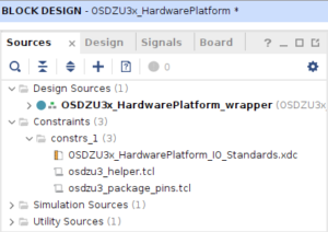

Constraints Files Loaded
Generating a Bit File
The generation of the hardware platform using the OSDZU3 Board Definition Files is now completed. You can now build the design and generate a bit file.
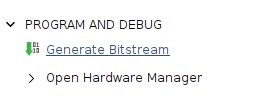
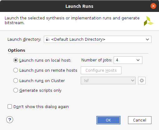
- Click on Generate Bitstream in Vivado GUI to generate a bit file for the hardware platform.

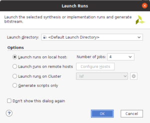
Generate Bitstream Button - When the following dialog box appears, click OK to continue.
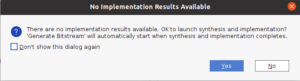
Dialog to click OK to proceed - When the following dialog box appears, click Yes to continue.

Dialog to select Yes

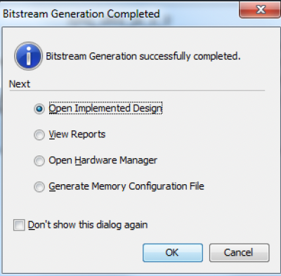
When the following dialog box appears, click OK to continue. This will open the implemented design in the Vivado GUI and you should see the device diagram. The implemented design needs to be open prior to exporting the hardware platform to Vitis.
Exporting the Hardware Platform
Now that the hardware platform has been generated, you can export it to Vitis in order to generate a Software Project (that includes a BSP) as well as all other software applications.
- With the Implemented Design Open in Vivado GUI, select File > Export > Export Hardware from the Vivado toolbar. The Export Hardware Platform window will open.
- Click Next
- Under Output -> Include bitstream
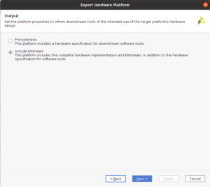

Example exporting the project - Choose XSA file name and export location
- Finish
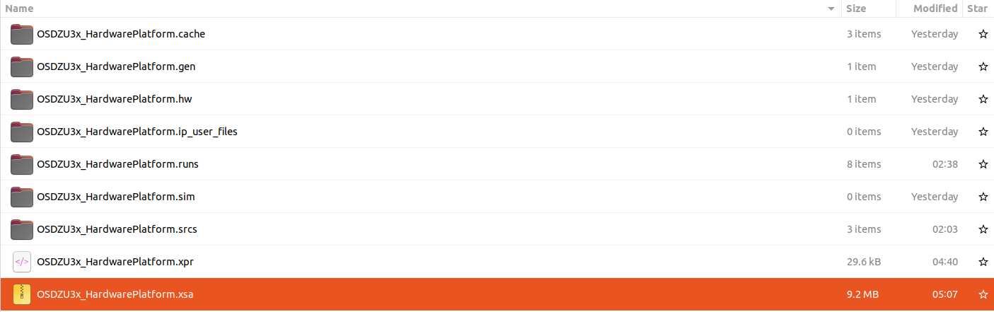
- The Vivado hardware platform file (.xsa) should now be available in the location chosen. It can be imported to Vitis, as necessary, to develop software applications on top of it.
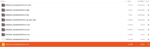
OSDZU3 hardware platform exported
Further Reading
To learn more about developing software applications on top of the newly created hardware platform using Vitis, refer OSDZU3-REF Vitis Tutorial.
Revision History
We will continue to update this application note to provide more information and more examples. Sign up below to be notified when we update this guide.
"*" indicates required fields
| Revision Number | Revision Date | Changes | Author |
| 1 | 12/20/2022 | Initial Public Release | Eshtaartha Basu |
