Terminating input power unused pins.
Forums › Devices › OSD335x-SM › Terminating input power unused pins.
- AuthorPosts
- February 7, 2022 at 2:04 pm #12045

 bpiquetteParticipant
WAY back in 2018 when we designed in the OSD3358-SM into our product, Rev 4 of the datasheet didn’t suggest grounding the unused VIN_USB pins or connecting VIN_BAT to PMIC_BAT_SENSE. I see that the most current rev of the datasheet is suggesting those connections, as well as your online schematic checklist.
What were the reasons for updating the documentation from what was the case back at Rev 4??
Were issues seen in designs that did not ground the VIN_USB? If yes, what behavior?I’ve got a small number of recently build devices at are exhibiting some intermittent power up behavior and am wondering if it is related.
- February 8, 2022 at 12:21 pm #12054
 Neeraj DantuModerator
bpiquette,
The recommendation was added based on section 9.2.2.2 of TPS65217C datasheet(https://www.ti.com/lit/ds/symlink/tps65217.pdf) and app note(https://www.ti.com/lit/an/slva901/slva901.pdf).
We have seen a customer see spikes at VIN_USB preventing the board from booting through VIN_AC. Please probe voltage at VIN_USB when you are powering the board to see if there grounding the USB is the problem in your use case.
Best,
Neeraj - February 11, 2022 at 12:43 pm #12057bpiquetteParticipant
Unfortunately, we did not include test points on this USB inputs pins, so probing will be hard.
Do you know of any other evidence to look for that would suggest that this is what is happening with our problem boards?
Apparently we have 3+ PCBAs that exhibit this problem fairly regularly (like 1 in 10 power cycles) but our customer has seen it on more of the devices that are in the field though less regularly.
- February 11, 2022 at 12:45 pm #12058bpiquetteParticipant
I suppose we would see that SYS_VOUT would not be as expected even if we have applied the VIN_AC?
- February 16, 2022 at 10:29 am #12061Neeraj DantuModerator
bpiquette,
Yes, please scope shot the behavior of SYS_VOUT when this faulty power-up happens. Do you have power draw measurements when the device exhibits this fault? If SYS_VOUT comes up fine, can you map out the power up sequence as shown in Figure 2 of the power application note: https://octavosystems.com/app_notes/osd335x-sm-power-application-note/?
Best,
Neeraj - February 23, 2022 at 6:55 pm #12081bpiquetteParticipant
Unfortunately we did not add a test point to the SYS_VOUT node so I don’t have access to it.
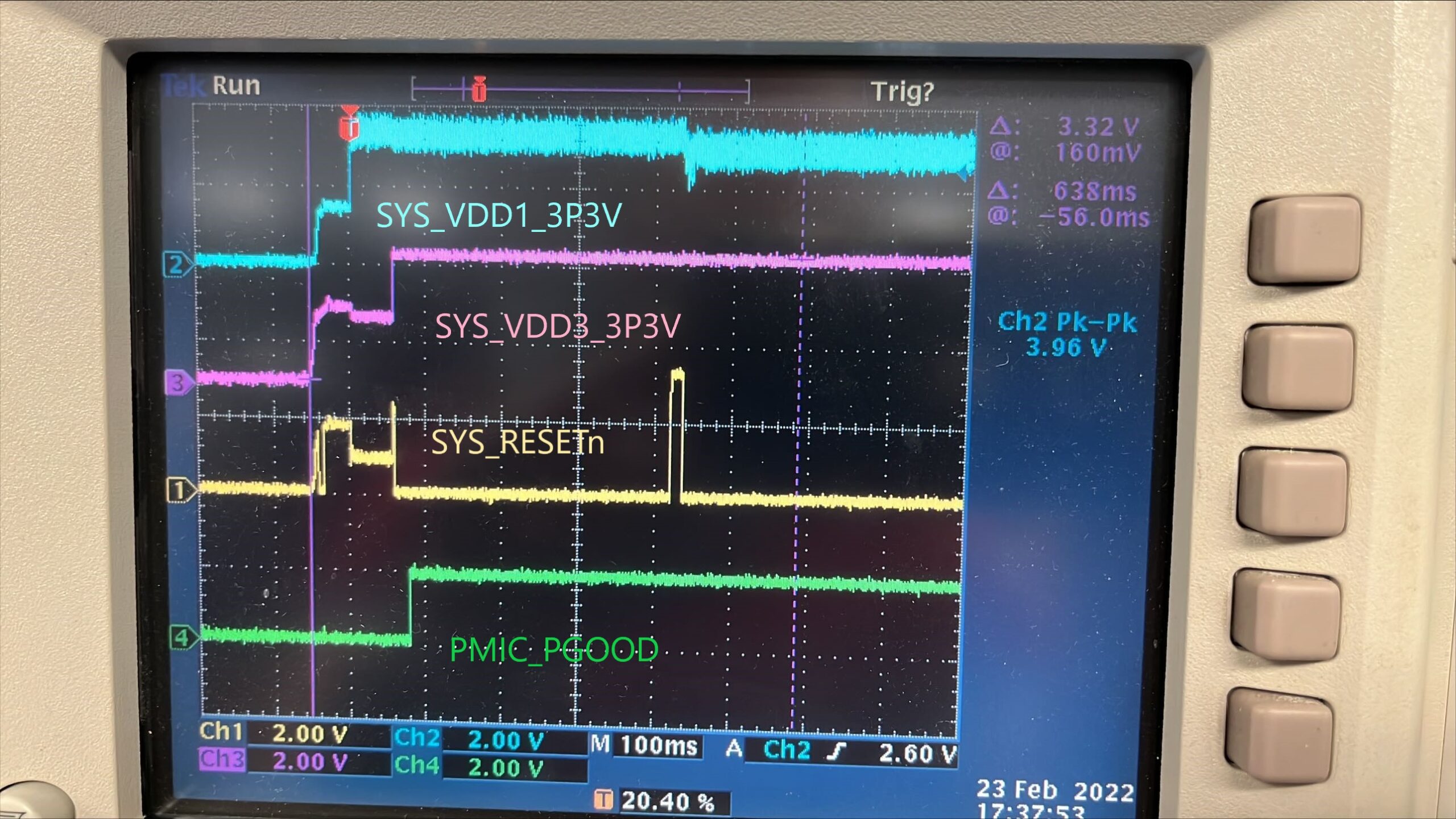
I see SYS_RTC_1P8V come up as expected even in this failure mode.We have discovered that when the PCBAs don’t boot, we see some excessive ripple on SYS_VDD1_3P3V (TL5209 output).
See attachments for comparison of good and bad power on.- This reply was modified 2 years, 2 months ago by
 bpiquette.
Attachments:
- This reply was modified 2 years, 2 months ago by
- February 23, 2022 at 6:57 pm #12083bpiquetteParticipant
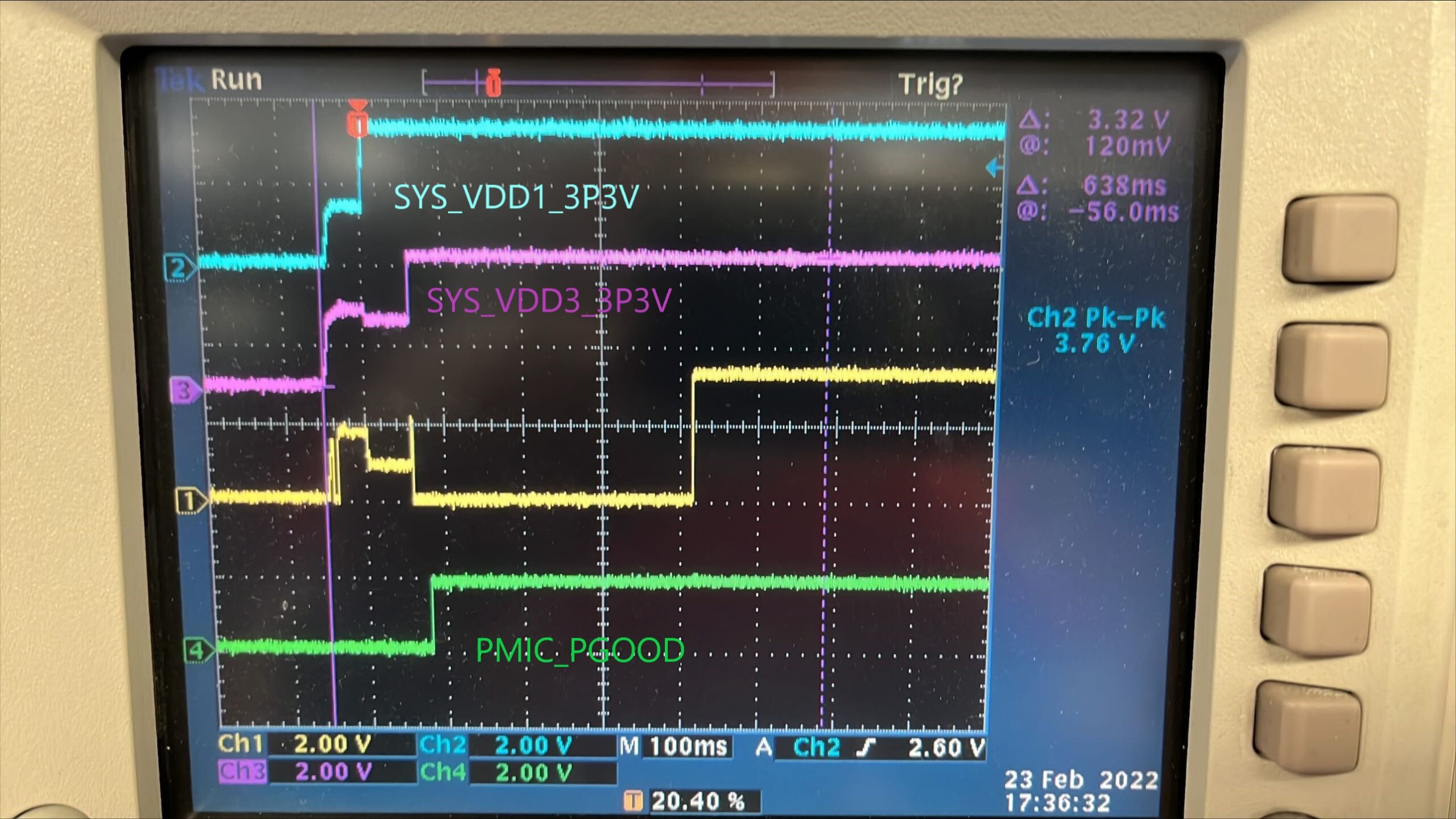
Example of good power on sequence
Attachments:
- February 27, 2022 at 5:57 pm #12099Neeraj DantuModerator
bpiquette,
Both sequences show PGOOD coming up and staying up, which says that PMIC thinks all power rails are good. VDD1_3P3V sags slightly at the point of failure indicating there is a device on this power rail that is drawing excess current(possibly responsible for faulty power up?).
Is your boot media powered by VDD1_3P3V? If so, is it possible to use another boot source changing the SYSBOOT pins? For example, you can bypass the current boot media and let the board boot up in UART boot mode. You will be able to see “CC” on the UART terminal. Does the fault still occur in this different boot mode?
How much bypass capacitance do you have on SYS_VDD1_3P3V? Can you increase it and see if the board behaves differently?
Can you also check whether the 24MHz and 32KHz oscillators are working correctly normally as well as in failure mode?
Best,
Neeraj
- AuthorPosts
- You must be logged in to reply to this topic.
