PinMux for OSD335x Family and AM335x SoC
Published On: January, 9, 2019 By: Neeraj Dantu | Updated: January 17, 2019 by Cathleen Wicks
Most microprocessors and microcontrollers have input or output (IO) pins that support different functionality, such as multiple communication protocols (e.g. UART, I2C, SPI, etc.), pulse width modulation (PWM), or general-purpose input and output (GPIO), depending on how they are configured. Configuring the functionality of a given multi-function pin, or pin multiplexing (PinMux), is an important part of the embedded design process. Determining the functionality of a given pin is one of the first stages in the embedded design process and forms a foundation for the rest of the design. For a Linux based Embedded System, there are multiple steps involved in configuring pin functionality and invoking proper pin functions during boot. This application note will describe the process of configuring pin multiplexing (PinMux) for the OSD335x System-in-Package (SiP) family as well as the PinMux for the AM335x SoC within it.
Table of Contents
1.Introduction
2.Revision History of this Document
3.Pin Multiplexing (PinMux) Overview
4.Pin Multiplexing for Linux Based Systems
5.Device Tree Overview
6.OSD335x Family Pin Multiplexing Device Tree Workflow
6.1Using the AM335x PinMux Tool
6.2Mapping AM335x Pins to OSD335x Pins
6.3Creating Device Trees
7. Conclusion
![]()
![]() A PDF version of this App Note can be found here.
A PDF version of this App Note can be found here.
2 Revision History
| Revision Number | Revision Date | Changes | Author |
|---|---|---|---|
| 1 | 1/17/2019 | Initial Release | N. Dantu |

3 Pin Multiplexing (PinMux) Overview
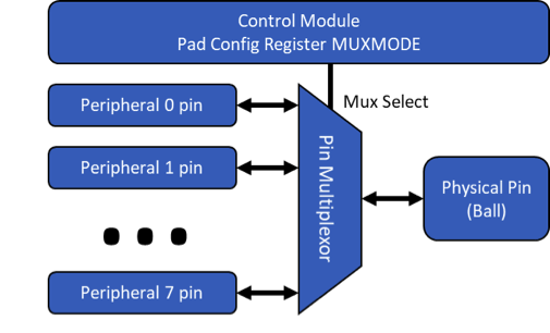
The Texas Instruments Sitara™ ARM® Cortex®-A8 AM335x System on a Chip (SoC) inside the OSD335x Family of devices has hundreds of IO pins. Each of these IO pins can have up to 8 different functions. Figure 1 shows a simplified block diagram of the AM335x pin multiplexing.
The possible functions of each pin can be found in the AM335x datasheet. Figure 2 shows part of the “Pin Attributes” table in the AM335x datasheet. This table provides important information, including the possible pin functions, for each pin. Note that the OSD335x SiP family contains AM335x die corresponding to the ZCZ package.
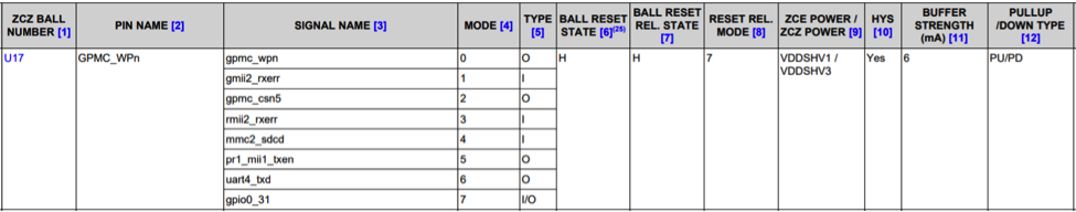
The “SIGNAL NAME” column lists the functional names the pin can be configured as using the corresponding “MODE” number. For example, the GPMC_WPN pin can be configured as the TXD pin for the UART4 peripheral by setting the MUXMODE field of the conf_gpmc_wpn Pad Control Register to a value of 6. All Pad Control Registers can be found in the Control Module (Memory Map Base Address: 0x44E1_0000) starting at offset 0x800 (See Chapter 9 of the AM335x Technical Reference Manual).
Along with the possible pin functions, the table also shows the IO voltage domain of the pin (i.e. “ZCZ POWER”), the reset state (i.e. “BALL RESET STATE”) and the reset release state (i.e. “BALL RESET REL.STATE”) of the pin. The IO voltage domain, i.e. VDDSHVx, of a pin is important because in some members of the OSD335x Family of devices, such as the OSD335x-SM and OSD335x C-SiP, the VDDSHVx pins are exposed allowing the user to select the IO voltage of the pin, either 1.8V or 3.3V operation. When setting an IO voltage domain, all pins within the IO voltage domain will be set to that operating voltage which is important when determining system connections with other components of the embedded design.
Similarly, the reset and reset release states of a pin are important to ensure that both the reset behavior and default pin behavior do not have any unintended consequences in the embedded design. For example, if the GPMC_WPN pin above is used an a GPIO enable for a component, then that component will be enabled by default since the reset and reset release states for that pin are “H” or a logic 1. This may or may not be the desired default system behavior and must be comprehended as part of the design.
Additionally, some of the IO pins, i.e. the SYSBOOT pins, are sampled on the rising edge of reset to determine the boot configuration of the AM335x processor. These pins must be pulled either high or low to set the appropriate boot configuration. This “default value” must also be comprehended as part of the embedded design to ensure that there are no system issues. For example, a SYSBOOT pin being used as a GPIO enable/disable for a chip may be pulled up/down for the boot mode setting, which if unnoticed can cause the board to exhibit unexpected behavior. The system designer must also ensure that there are no additional pull up or pull down resistors on the SYSBOOT pins that could alter the sampled boot configuration value. For example, if SYSBOOT[0] was required to be sampled low to set the proper boot mode but was used with a system component that required a strong pull up, this could lead to the AM335x not booting properly.
4 Pin Multiplexing for Linux Based Systems
The Linux kernel is a versatile software component that can run on a wide variety of embedded processors and embedded designs. While some things, such as the processor architecture, are specified during the kernel build process, other things, such as the custom printed circuit board (PCB) level pin configuration, should not be built into the kernel itself since that would dramatically increase the size of the kernel. Instead, a separate binary is passed to the kernel that describes the hardware on the PCB and pin configuration of the processor. The binary is called a device tree blob (dtb)which is built from a device tree source (dts). Among other things, a device tree supplies the following information to the Linux kernel:
- Pin multiplexing
- Drivers to be invoked
- Peripheral register memory map addresses and lengths in the processor
- Property values to be set
Before diving into the workflow around setting pin multiplexing for the OSD335x Family of devices, it is important to first have a good understanding of Linux device trees.
5 Device Tree Overview
At the core the device tree is a data structure. The following example device tree block diagram shows the organization of the structure.
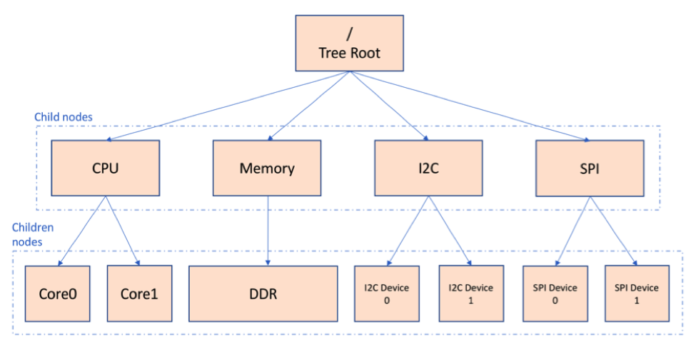
A typical device tree contains the CPU and memory nodes describing each cpu and memory in the corresponding child nodes. As described above, peripheral specific driver invocation and configuration is done in the corresponding node of the peripheral.
More information on device tree structure and configuration can be found in the following places:
- Series of three application notes for getting started with OSD335x and Linux Device Tree: https://octavosystems.com/2018/07/12/leveraging-linux-enlightened-under-the-tree/
- Device Tree for Dummies: https://events.static.linuxfound.org/sites/events/files/slides/petazzoni-device-tree-dummies.pdf
- Device Tree Specification: https://github.com/devicetree-org/devicetree-specification/releases/tag/v0.2
- Device Tree usage: https://elinux.org/Device_Tree_Usage
- Linux Kernel Device Tree Bindings: https://git.kernel.org/pub/scm/linux/kernel/git/torvalds/linux.git/plain/Documentation/devicetree/bindings
6.0 OSD335x Family Pin Multiplexing Device Tree Workflow
There are many workflows when it comes to using the device tree to configure the IO pins of the OSD335x Family of devices for an embedded design. The following procedure describes one workflow that can be used for the OSD335x Family of devices.
First, a designer can use the PinMux tool provided by Texas Instruments to map the required peripherals to appropriate AM335x pins. Then, the designer can map the AM335x pin to the appropriate OSD335x device pin using the Octavo Systems provided app note in order to create design schematics. At the same time, the designer can use the AM335x pin mapping to generate the necessary Linux device tree infrastructure. One thing to note is that the software required to configure a given pin is the same between the AM335x and any of the OSD335x devices even though the physical location of that pin may be different.
6.1 Using the AM335x PinMux Tool
Once a system designer has created the basic block diagram of the embedded system, a pin map should be created that will map each of the AM335x IO pins to the other components of the system. Texas Instruments provides a Pinmux tool (https://dev.ti.com/pinmux/) to help map the peripherals of the AM335x to the appropriate IO pins. A web account with ti.com is needed to access this tool. Additional resources including a getting started video can be found on the TI PinMux Tool wiki.
Figure 4 shows the tool start page. The “Device” field needs to be set to “AM335x” and the “Package” field needs to be set to “ZCZ” before starting the tool.
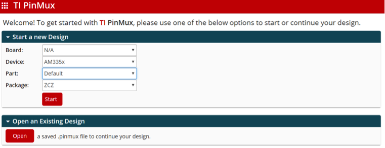
Figure 5 shows the PinMux Tool layout. All the peripheral interfaces of the AM335x are listed on the left-hand side. Peripherals can be added in and configured in the “Requirements” menu.
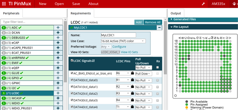
Each pin of a peripheral can be assigned to an appropriate AM335x pin using the pulldown menu in the “Pins” column. However, there is one caveat when assigning a peripheral interface to a given set of AM335x pins: All the pins of the peripheral need to be part of defined IO Set (i.e. not all combinations of pins for a given peripheral are allowed). Only the peripheral pins in a given IO Set are guaranteed to meet the timings specified in the datasheet. All the IO sets for a peripheral can be viewed by clicking on the “View IO Sets” link in the “Requirements” section of the PinMux Tool.
It is also important to avoid pin conflicts (i.e. trying to use the same physical pin for 2 different functions) when selecting the IO Set for a peripheral. The PinMux Tool will highlight any conflicts that arise during the pin selection process. After adding all the peripherals including ones used inside the SiP and selecting the proper IO sets, a functional pin map of the SoC is generated. This functional pin map will allow you to configure pins appropriately in the device tree.
6.2 Mapping AM335x Pins to OSD335x Pins
Once the peripheral pins have been successfully mapped to the AM335x pins, in order to create schematics, it is necessary to translate the AM335x physical pin (ball) to the OSD335x physical pin (ball). This can be done easily using the pin mapping table available here:
https://octavosystems.com/app_notes/am335x-signal-to-osd335x-pins/
For example, assume that the embedded design using the OSD335x C-SiP requires the use of the UART1 peripheral. First, the designer will use the PinMux Tool to select the AM335x UART1 pins, as seen in Figure 6.
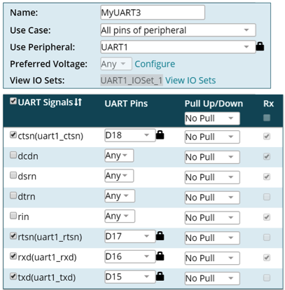
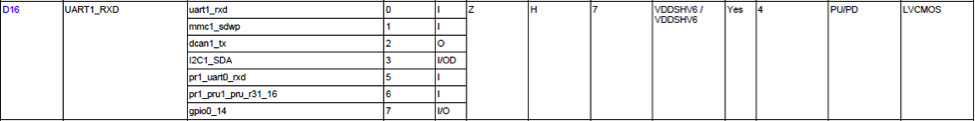
As one can see, the UART1 interface uses four AM335x pins belonging to the same IO set which do not conflict with other peripheral pins of the design, i.e. AM335x pins D15, D16, D17 and D18. With this information, the designer can then use the pin mapping spreadsheet to translate these pins into the appropriate OSD335x pins, as seen in Figure 7.
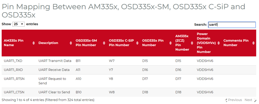
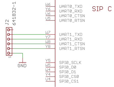
Since this design uses OSD335x C-SiP, we can match the pin in the “AM335x (ZCZ) Pin Number” column to the pin in the “OSD335x C-SiP Pin Number” column. Hence, the pins D15, D16, D17 and D18 are mapped to the pins W7, Y7, Y8 and W8, respectively. This then allows the designer to create the proper schematic connections for UART1, as seen in Figure 8.
Some additional things to note as part of this translation process:
- The “AM335x Pin Name” column in the pin mapping spreadsheet corresponds to the “PIN NAME” column in the AM335x datasheet (see Figure 2) and may or may not reflect the actual function of the pin.
- In general, the OSD335x pin name matches the AM335x pin name, except where noted in the datasheet.
- All IO pins of the AM335x ZCZ package are available on the OSD335x devices, except in the OSD335x C-SiP where some of the GPMC pins are used within the SiP to connect to the eMMC (see OSD335x C-SiP datasheet for more information).
- The DDR (EMIF) interface is not available on the OSD335x devices because the DDR memory is integrated within the OSD335x devices.
6.3 Creating a Device Tree
After all the peripheral pins have been selected using the AM335x Pinmux Tool, a designer can also create a Linux device tree to appropriately configure all of the pins for proper operation within the system. While the AM335x pin name might not accurately reflect the function of a given pin, it is important to understand this name because it will be used as the pin identifier in all AM335x and OSD335x documentation. While a device tree can be written from scratch, it is usually easier to start with a known working device tree and modify it to reflect the new system design.
There are many example device trees that have been created around the AM335x processor within the OSD335x. One example is incorporated in the OSD3358-SM-RED Reference, Evaluation, Development Board for the OSD335x Family. The device tree source files for OSD3358-SM-RED are provided at:
https://github.com/octavosystems/OSD335x-Device-Tree
Similarly, example device trees created around the BeagleBoard.org ® family of products can be found in the src/arm directory of Robert Nelson’s Device Tree Rebuilder:
https://github.com/RobertCNelson/dtb-rebuilder
The Device Tree Rebuilder project can also be used to easily build device tree blobs (dtb) from device tree source (dts) files.
Continuing the above example, the new OSD335x C-SiP embedded design needs to use the UART1 peripheral. Therefore, the designer can start with the OSD3358-SM-RED device tree (osd3358-bsm-refdesign.dts) and modify it to enable UART1 and have it use the pins that were previously selected. Before modifying the device tree, it is important to understand the current definition of UART1 in the device tree. Looking through the device tree source (dts) file and all device tree source include (dtsi) files referenced in the device tree source, the designer can see that the UART1 definition is (see osd335x-sm.dtsi):
1 2 3 4 5 6 7 8 9 10 | uart1: serial@48022000 { compatible = "ti,am3352-uart", "ti,omap3-uart"; ti,hwmods = "uart2"; clock-frequency = <48000000>; reg = <0x48022000 0x2000>; interrupts = <73>; status = "disabled"; dmas = <&edma 28 0>, <&edma 29 0>; dma-names = "tx", "rx"; }; |
From this definition, the designer can see that the peripheral is currently “disabled” (i.e. the status property is set to “disabled”) and does not have any pin multiplexing information defined. Therefore, in this device tree, the designer must:
- Set up the pin multiplexing for the embedded design
- Enable the peripheral
If there was already pin multiplexing defined, then the designer would just need to modify the existing pin multiplexing. However, given there is no pin multiplexing defined, the designer first must declare the pins that should be used with the peripheral. This can be done by adding a sub-block for the uart1_pins to the am33xx_pinmux node within the device tree:
1 2 3 4 5 6 7 8 9 10 11 12 | &am33xx_pinmux { <Other Pin Definitions> uart1_pins: pinmux_uart1_pins { pinctrl-single,pins = < AM33XX_IOPAD(0x984, PIN_OUTPUT_PULLDOWN | MUX_MODE0) /* uart1_txd.uart1_txd */ AM33XX_IOPAD(0x980, PIN_INPUT_PULLUP | MUX_MODE0) /* uart1_rxd.uart1_rxd */ AM33XX_IOPAD(0x978, PULL_DISABLE | MUX_MODE0) /* uart1_ctsn.uart1_ctsn */ AM33XX_IOPAD(0x97c, PIN_INPUT_PULLUP | MUX_MODE0) /* uart1_rtsn.uart1_rtsn */ >; }; <Other Pin Definitions> }; |
In the uart1_pins block, there are a number of items that need to be understood to fully comprehend what this definition is doing. First, there are many AM335x specific macros that are used which have been defined as part of the device tree bindings (files such as include/dt-bindings/pinctrl/am33xx.h or include/dt-bindings/pinctrl/omap.h which can be found in the Device Tree Rebuilder). These include “AM33XX_IOPAD”, “MUX_MODE0”, “PIN_INPUT_PULLUP”, etc. In order to correctly configure the pin multiplexing, the pinctrl-single,pins entry of the device tree really just needs a list of numbers pairs: <address offset> <register value>. This can be seen in other device trees, such as the am335x-boneblue.dts:
1 2 3 4 5 6 7 8 9 10 11 | &am33xx_pinmux { /*************************************************************************** * Static Pinmux ***************************************************************************/ mux_helper_pins: pins { pinctrl-single,pins = < /* GPIO Inputs */ 0x09c 0x37 /*P8.9 Pause BUTTON, input pullup*/ 0x098 0x37 /*P8.10 MODE BUTTON input pullup*/ 0x1AC 0x37 /*P9.25 MPU-9150 INTERRUPT IN*/ ... |
However, the macros make it easier for people to understand how the pins are being configured. Breaking down the line:
1 | AM33XX_IOPAD(0x984, PIN_OUTPUT_PULLDOWN | MUX_MODE0) /* uart1_txd.uart1_txd */ |
The number 0x984 refers to the address offset within the Control Module of the uart1_txd Pad Control Register (see the AM335x Technical Reference Manual for more information):
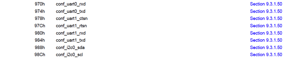
Again, the name used for the register is the same as the “PIN NAME” defined in the datasheet and does not necessarily correspond to the actual functionality of the pin. The “MUX_MODE0” macro refers the peripheral that will use this pin:
The “PIN_OUTPUT_PULLDOWN” macro refers to the configuration of the “RXACTIVE”, “PULLTYPESEL”, and “PULLUDEN” fields within the Pad Control Register (See Section 9.2.2 of the AM335x Technical Reference Manual).
Finally, the “AM33XX_IOPAD” macro converts the inputs to the format that is needed for the pinctrl-single,pins entry of the device tree. As n side note, the address offset required for the pinctrl-single,pins entry is the Control Module register address offset minus 0x800. For example, in the am335x-boneblue.dts snippet above, the number 0x09c refers to the Pad Control Register conf_gpmc_ben0_cle which is at Control Module address offset 0x89c.
It is important to make sure that there are not conflicting pin multiplexing assignments present in either the device tree source file or any device tree source include files that are referenced.
Once the pin multiplexing entry has been added, the uart1 device tree node can be referenced and the properties updated to enable the peripheral and associate the pin multiplexing entry. This can be done by adding the following to the device tree source file:
1 2 3 4 5 | &uart1 { pinctrl-names = "default"; pinctrl-0 = <&uart1_pins>; status = "okay"; }; |
In this definition, the designer can see that UART1 has been enabled by setting the “status” property to “okay”. Additionally, the “pinctrl-0” property is set to the “uart1_pins” sub-block that was added to the “am33xx_pinmux” to map the peripheral pins to the appropriate device pins.
Once the device tree source (dts) has been modified, a new device tree binary (dtb) can be built and used in the new embedded system. The following procedure provides an overview for the building and using the new device tree (This procedure assumes the file organization that is found the in the Linux images provided by BeagleBoard.org®):
- Download or clone the dtb-rebuilder (https://github.com/RobertCNelson/dtb-rebuilder)
- Copy the updated device tree source and all necessary include files to the /src/arm directory
- Use the make command to build the device tree binary
- A .dtb file with the same name as the .dts file is generated during the build process
- Copy the .dtb file to the /boot/dtbs/<kernel version>/ directory in your Linux image to make it available to the Linux Kernel during boot
- Configure the boot configuration file (txt) to use the new device tree:
- Open the /boot/uEnv.txt file using a text editor, like nano: nano /boot/uEnv.txt
- Comment out the existing dtb variable and add the line: dtb=<your-dtb-file-name>.dtb
- Save the file
- Reboot the system to have Linux boot with the new device tree
- The example updates made to the device tree to enable and connect UART1 will generate a UART dev interface file /dev/ttyO1 and communicate with a UART device attached to the OSD335x C-SiP pins W7, Y7, Y8 and W8.When using the above procedure:
- The device tree rebuilder version should match the Linux kernel version being used
- Any errors in syntax can be debugged using error messages they generate during compilation
Pin control definitions and modes can be found here: https://github.com/RobertCNelson/dtb-rebuilder/blob/4.14-ti/include/dt-bindings/pinctrl/am33xx.h
7 Conclusion
This application note provides an introduction to pin multiplexing on the AM335x and describes a process for managing the pin multiplexing for the OSD335x Family of System-in-Package devices. While one workflow is described, this is by no means the only way to perform pin multiplexing and this information can be tailored to the specific needs of the embedded system. Any corrections, clarifications, or questions on this application note can be posted on the Octavo Systems Forums.
