Vitis AI Tutorial – Part 1
Published On: November, 13, 2023 By: Eshtaartha Basu
This tutorial will walk you through the steps required to enhance your existing Hardware Platform in Vivado and make it Acceleration Ready. The Acceleration Ready Viavdo hardware platform, together with Vitis GUI and Vitis-AI framework (discussed in Vitis-AI Tutorials Part 2, Part 3 and Part 4), will help you offload specialized intensive software functions (related to AI, ML, Deep Learning etc) to an Acceleration Kernel in the PL. We will be using the OSDZU3-REF’s Vivado Hardware Platform as an example starting point.
This tutorial can be used standalone or as Part 1 of a 4-part Acceleration tutorial series that will help you run Vitis-AI DPU-TRD based Face Detection demo, ADAS Detection demo (and other AI demos) on the OSDZU3-REF board. An overview of the flow is shown below:
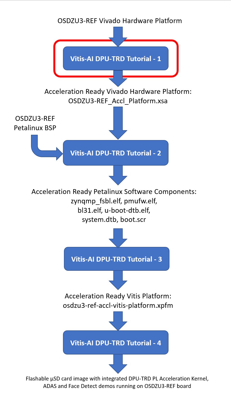
Table of Contents
Pre-requisites
This tutorial assumes the user is already familiar with the OSDZU3-REF Vivado and Vitis Design Flow by going through:
Objectives
To make the existing Vivado Hardware Platform Acceleration Ready, the user needs to create and make the following available to be used later by PL Acceleration Kernel:
- Add necessary clock, interrupt and other supporting IPs to the block design
- Perform Platform Setup to choose and enable clock outputs, interrupt channels and interfaces between PS and PL for acceleration
- Export Hardware
Tutorial Requirements
This tutorial will require the following software setup.
- Xilinx Vivado v2021.2 (Xilinx account and licenses may be required)
- When running the installer, ensure the Install Cable Drivers option is enabled.
- Ensure this Xilinx patch is applied to your Vivado installation before proceeding further with this app note: https://support.xilinx.com/s/article/76960?language=en_US
- OSDZU3-REF Vivado Hardware Project provided by Octavo Systems
- Download, import the project into your Vivado workspace and open it before proceeding with this tutorial.

Add IP Blocks to Enable Acceleration
The following sections will describe the various steps required to make the existing Vivado Hardware Platform Acceleration ready.
Before proceeding with new IP additions:
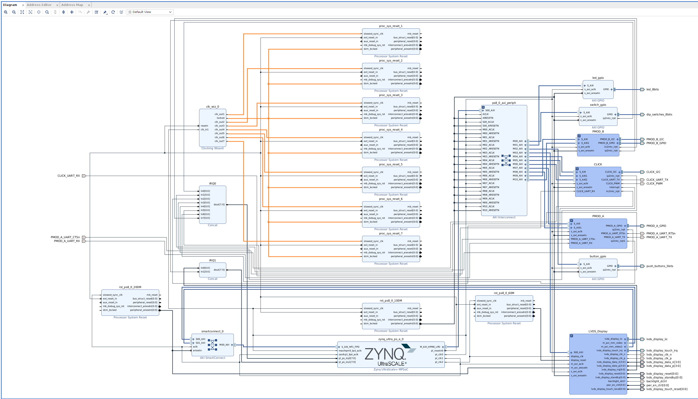
- Open OSDZU3-REF Vivado Hardware Platform
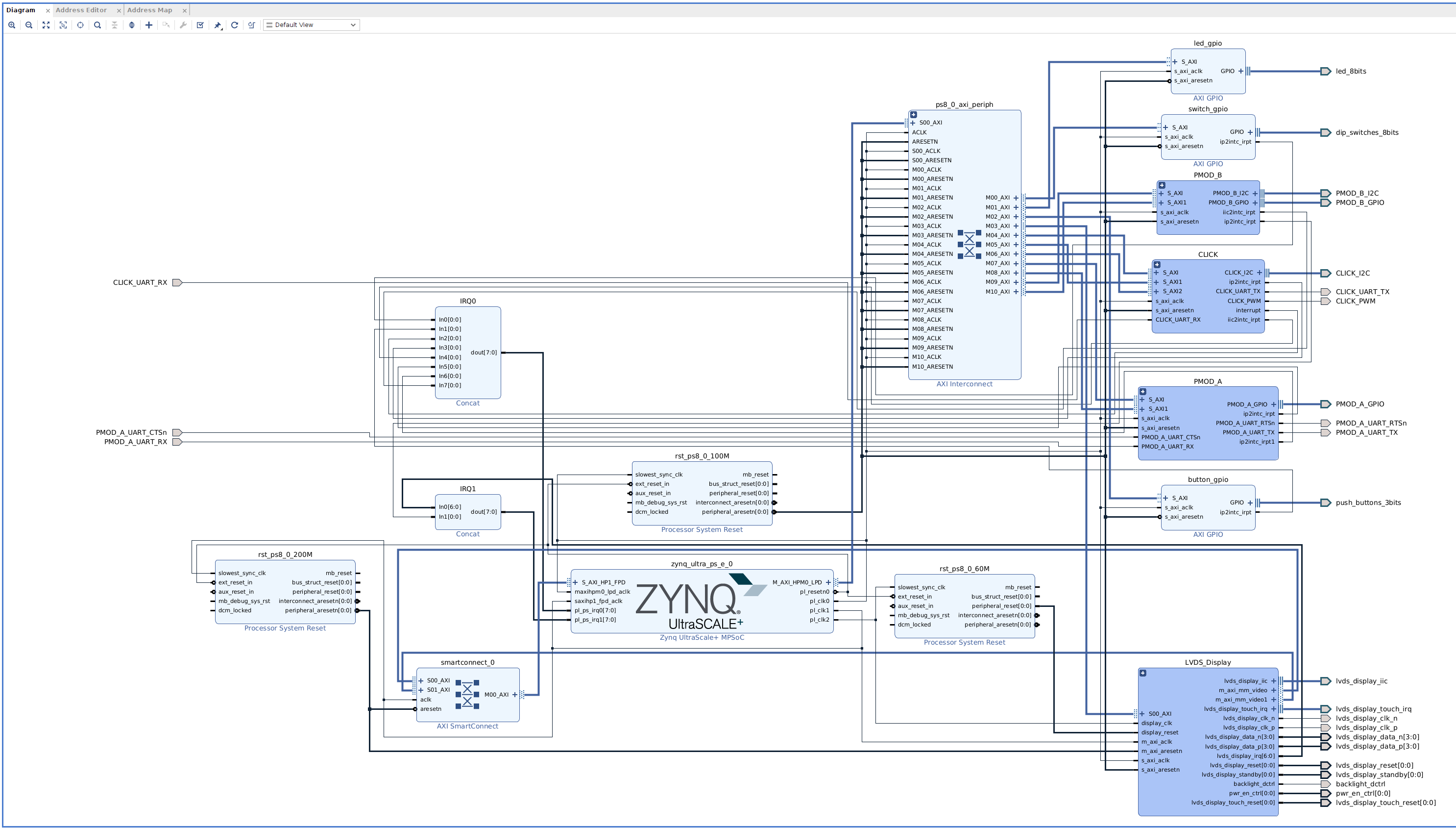
- Open Block Design. It should look similar to the picture below.
Add Clock Wizard
The processor’s pl_clk output can provide a maximum of 4 clock outputs and their phase is not aligned. To have the flexibility of multiple phase aligned clock outputs, add Clocking Wizard to the block diagram as follows:
- Right click on empty space in block design > Add IP
- Search for Clocking Wizard and add it.
- Double click on clk_wiz_0
- Under Output Clocks tab, enable 7 clock outputs from clk_out1 to clk_out7. Set the Requested Output Freq as shown below.
- Set Reset Type to Active Low > Click OK


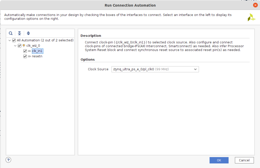
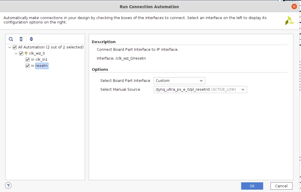
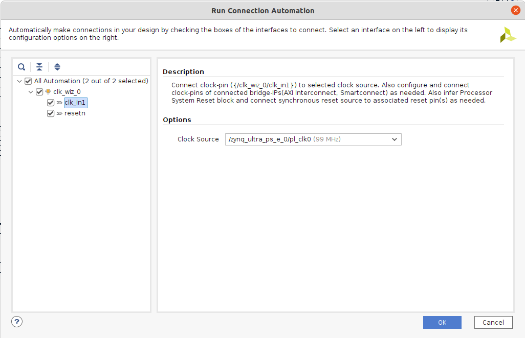
- Click on Run Connection Automation.
- In the Run Connection Automation Dialog Box,
- Choose pl_clk0 as input for clk_in1
- Choose pl_resetn0 as input for resetn
- Click OK


- This concludes the Clock Configuration for the Accelerated Design.
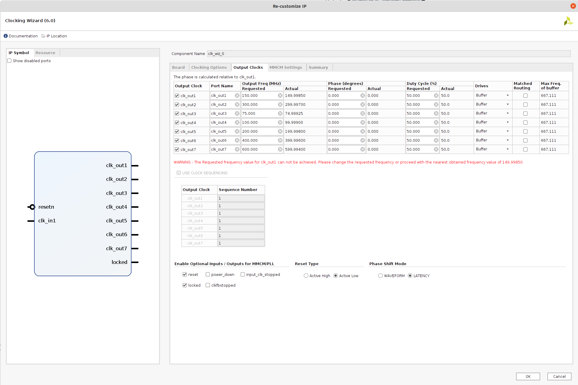
Among the above output clocks, we will be using 150MHz and 300MHz clock outputs as DPU AXI interface clock and DPU core clock respectively as part of Vitis-AI Tutorial Part – 4 (TBD link). Other clocks are made available for future flexibility.
Note: Feel free to modify the number of clock outputs and their frequencies to match your target design.
Add Processor System Reset blocks
Add Processor System Reset blocks for each of the clock outputs of the clock wizard. This is required for Platform Setup discussed later in this tutorial.
- Right click on empty space in block design > Add IP
- Search for Processor System Reset and add it.
- Duplicate the Processor System Reset IP six times by copying and pasting it and name the new IP blocks as proc_sys_reset_1, proc_sys_reset_2 up to proc_sys_reset_7 to match their names to the clock output numbers they will be connected to.
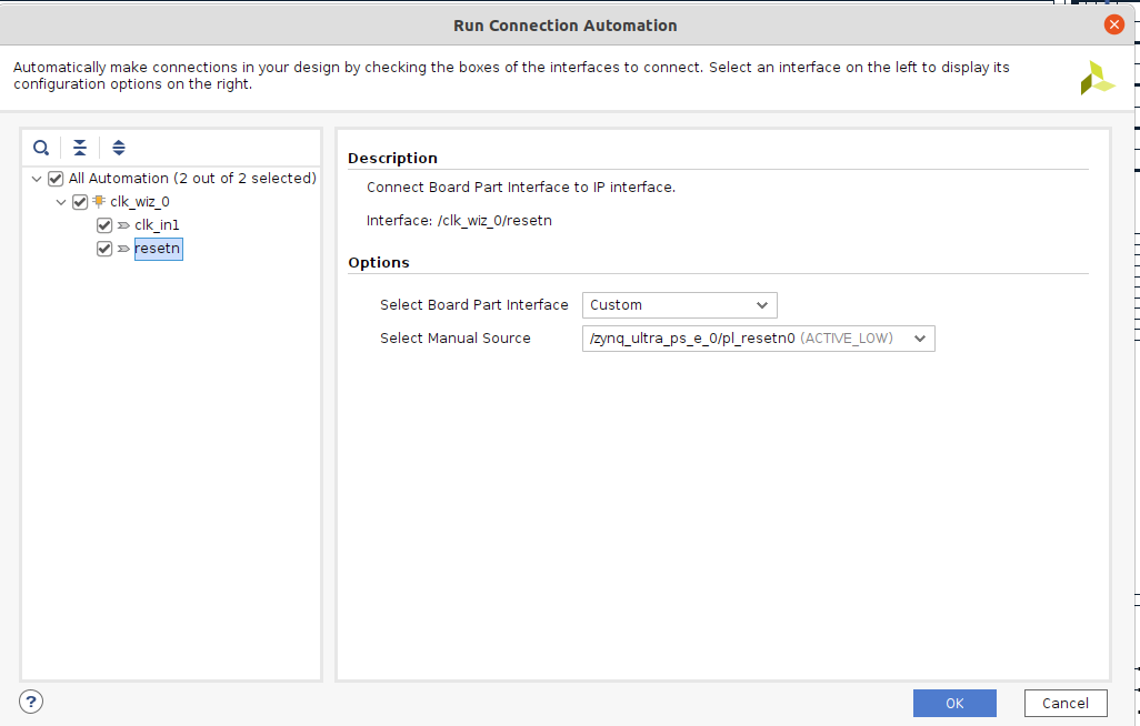
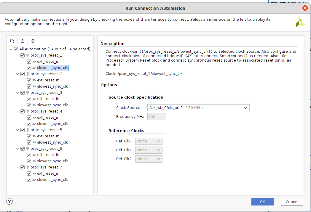
- Click on Run Connection Automation
- Enable All Automation on the left side of the Run Connection Automation window.
- For each of the proc_sys_reset IP blocks, set the Clock Source for slowest_sync_clk as listed in the table below.


Processor System Reset IP Clock source proc_sys_reset_1 /clk_wiz_0/clk_out1 (150MHz) proc_sys_reset_2 /clk_wiz_0/clk_out2 (300MHz) proc_sys_reset_3 /clk_wiz_0/clk_out3 (75MHz) proc_sys_reset_4 /clk_wiz_0/clk_out4 (100MHz) proc_sys_reset_5 /clk_wiz_0/clk_out5 (200MHz) proc_sys_reset_6 /clk_wiz_0/clk_out6 (400MHz) proc_sys_reset_7 /clk_wiz_0/clk_out7 (600MHz) - For each of the proc_sys_reset IP blocks:
- Set the Board Part Interface to Custom
- Set Select Manual Source to /zynq_ultra_ps_e_0/pl_resetn0
- Ensure all checkboxes are enabled in the window > Click OK to automatically create connections in the block design.
- Manually connect the dcm_locked signals of each of the proc_sys_reset instances to the locked signal on clk_wiz_0.
- Once the clock and reset connections are finished, the block diagram should look similar to what is shown below.


Add Interrupts
The processor’s pl_ps_irq can provide a maximum of 16 interrupts. To be able to handle more interrupt signals, add AXI Interrupt Controller as described below.
- Right click on empty space in block design > Add IP
- Search for AXI Interrupt Controller and add it.
- Double click on axi_intc_0
- Under Processor Interrupt Type and Connection, set Interrupt Output Connection to Single.
- Click OK.
- In the OSDZU3-REF block design, all the 16 interrupt signals are already occupied. To free up 1 interrupt signal for our newly added interrupt controller:
- Click on switch_gpio IP block > Uncheck Enable Interrupt check box. This will free up In0 input of IRQ0 Concat block.
- Connect the irq output of axi_intc_0 to In0 of IRQ0.
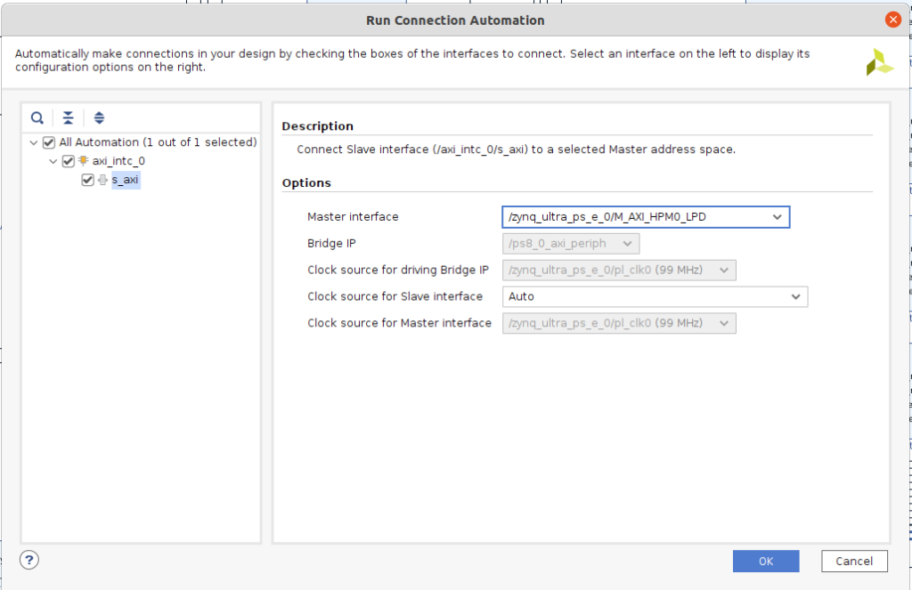
- Run Connection Automation
- Enable All Automation
- Click on s_axi.
- Set Master interface to /zynq_ultra_ps_e_0/M_AXI_HPM0_LPD
- Ensure all other settings are as shown below.

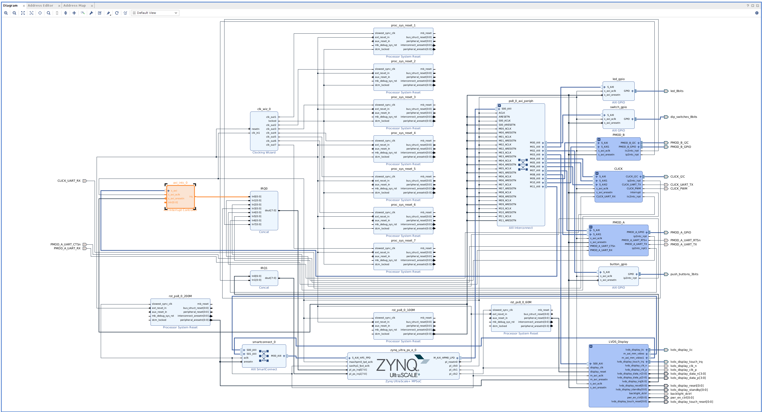
- This completes the interrupt setup. The block diagram should look similar to what is shown below.


Ensure correct PS-PL interface configuration
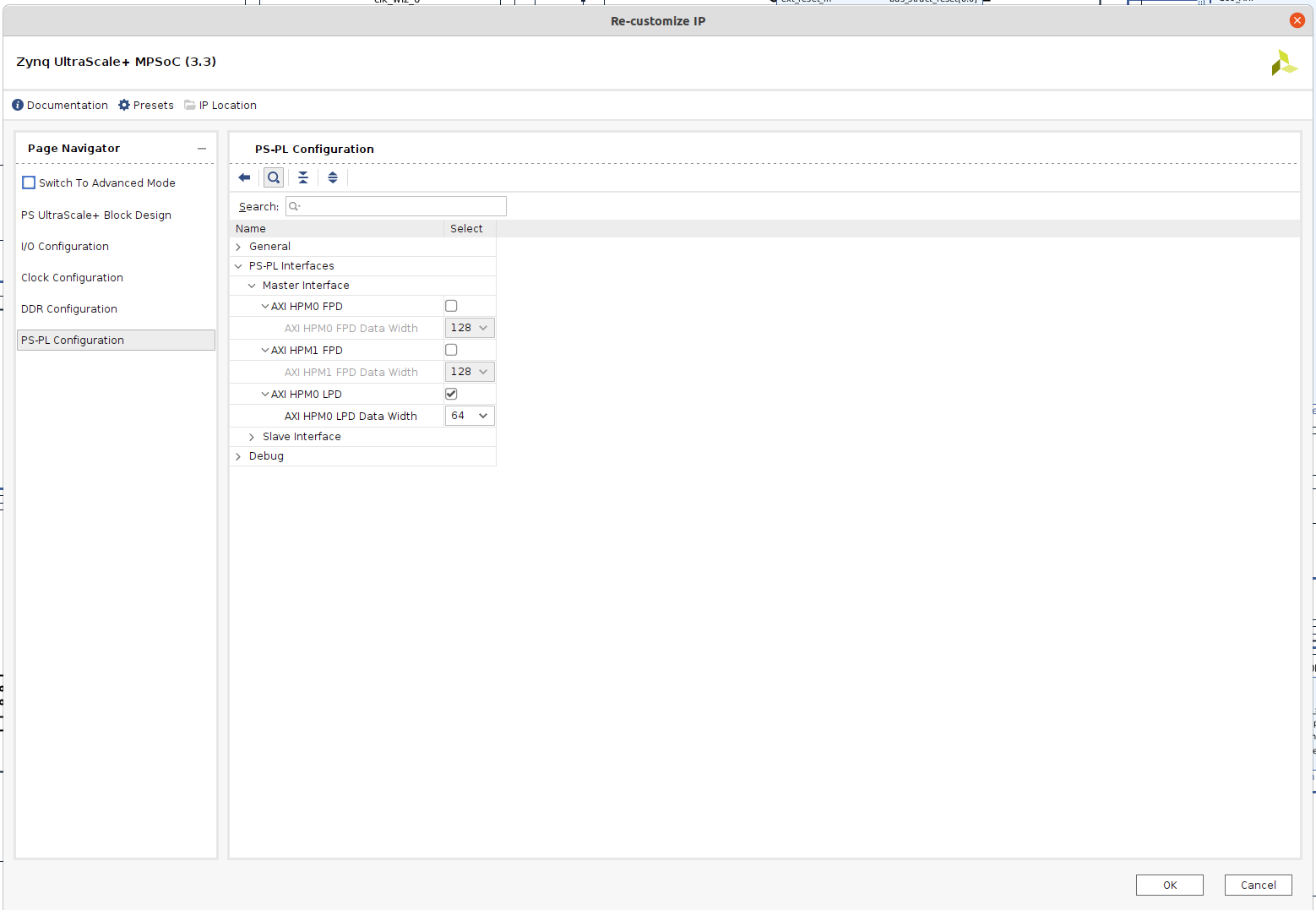
- Double click on zynq_ultra_ps_e_0 IP block
- Under Page Navigator, select PS-PL Configuration
- Under PS-PL Interfaces drop-down menu, ensure only AXI_HPM0_LPD is selected as shown below.
- AXI_HPM0_FPD and AXI_HPM1_FPD should be un-selected so that they’re reserved for PL acceleration kernel.
Platform Setup
Make the Vivado project an Extensible Vitis Platform
- Under Vivado Project Manager:
Go to Settings > Project Settings > General > Enable Project is an extensible Vitis platform as shown below.
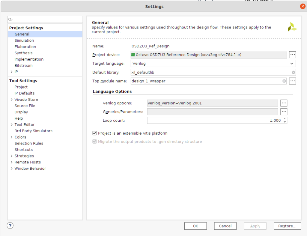

- Open Platform Setup under Window > Platform Setup.

Note: The Platform Setup window option appears only if the project is declared as an Extensible Vitis Platform as shown above.
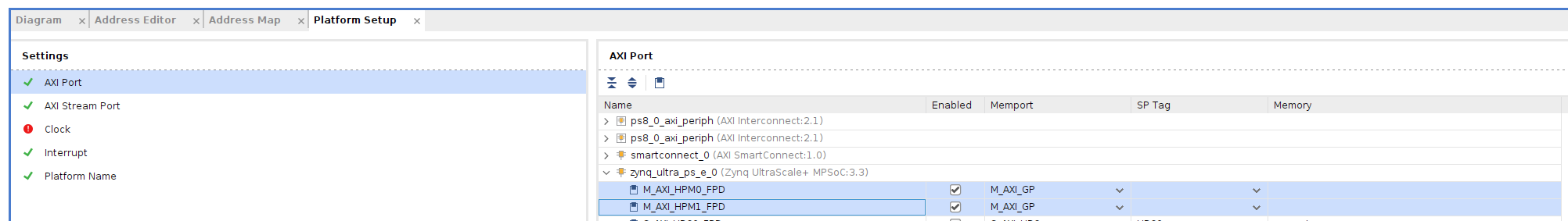
Enable PS AXI Master Interfaces
- Under Platform Setup, select AXI Port
- Under zynq_ultra_ps_e_0
- Enable M_AXI_HPM0_FPD
- Enable M_AXI_HPM1_FPD
- Under ps8_0_axi_periph
- Enable 7 interfaces from M12_AXI to M18_AXI
- Under zynq_ultra_ps_e_0
Note:
- The v++ linker will automatically connect PS AXI Master interfaces to PL’s Acceleration Kernals. One PS AXI master interface can connect with up to 16 slave PL kernels.
- SP tag is used only for AXI Slave Interfaces
- Exporting AXI master interfaces from AXI interconnect IP (I.e., ps8_0_axi_periph) will prevent v++ linker from automatically cascading to another level of AXI interconnect.
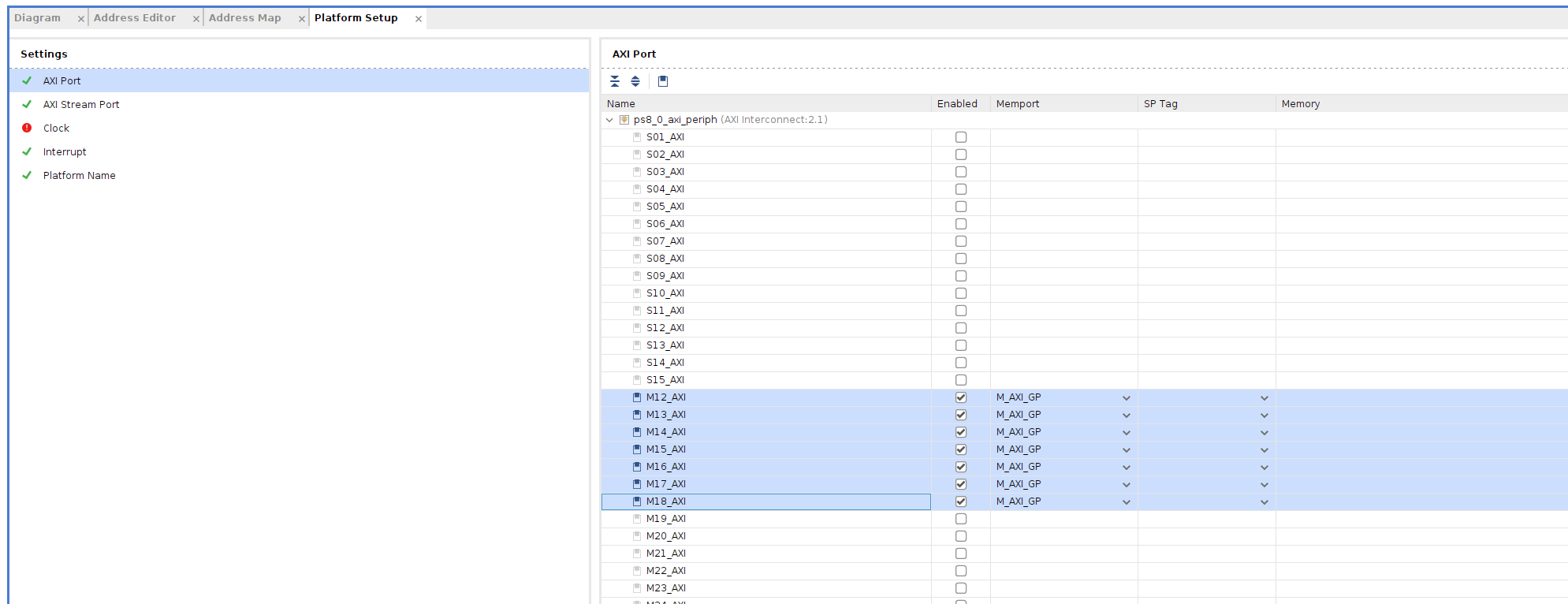
Enable PS AXI Slave Interfaces
PS AXI Slave Interfaces will allow PL Acceleration Kernel to access DDR memory.
- Under zynq_ultra_ps_e_0, enable all the AXI slave interfaces.
- Make sure to add sptag names as shown below.
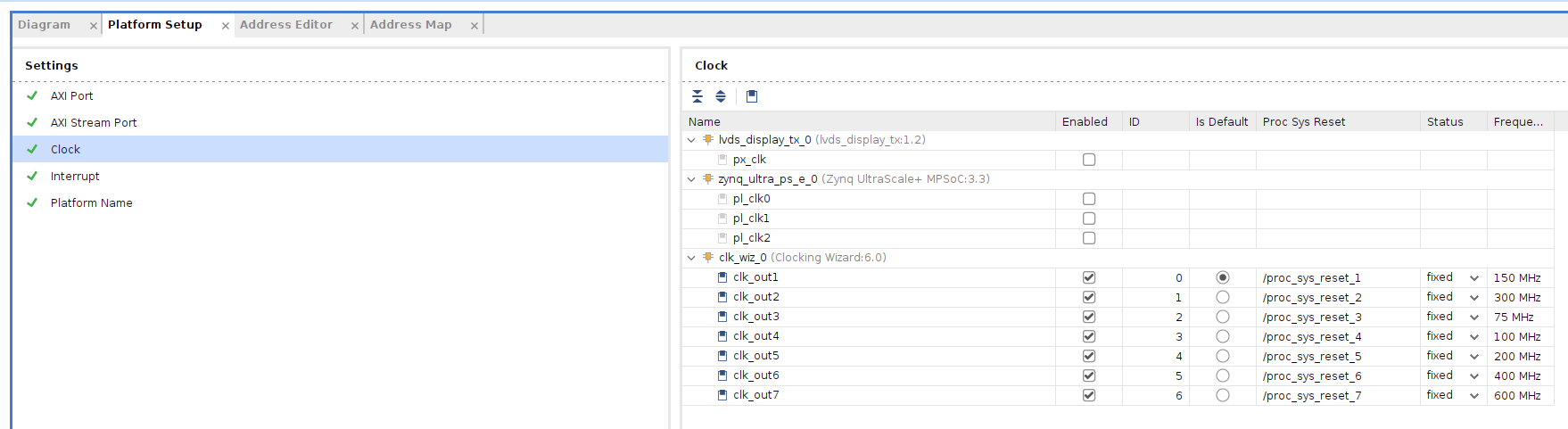
Enable Clocks
Under Platform Setup:
- Enable all clocks from clk_out1 to clk_out7
- Change the clock IDs to range from 0 to 6
- Set clk_out1 as default
- You should see a green tick next to the clock name in the left panel of platform setup. This indicates that there are no problems with clock interfaces.
Enable Interrupts
Under Platform Setup:
- Select interrupt tab
- Under axi_intc_0, enable intr.
Export Hardware
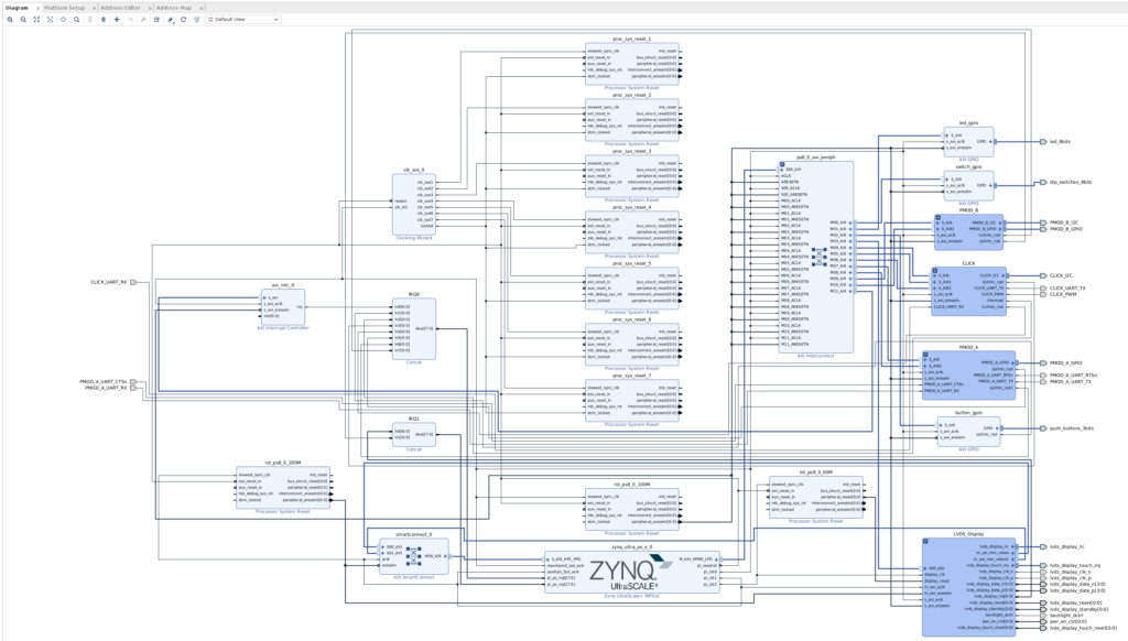
- Ensure your block diagram looks correct and satisfies your design needs. After adding and configuring all the IP blocks and interfaces as described in the previous sections, the overall block diagram should look similar to what is shown below.

- Right click on empty space in block diagram window -> Validate Design
- After validation, Vivado may throw the below critical warning indicating the intr input of axi_intc_0 IP block is floating. This warning can be safely ignored because the intr input will be suitably connected by v++ linker later while integrating PL Acceleration Kernel Interrupts with the platform.
- Under Vivado’s flow navigator on the left > Under IP Integrator > Click Generate Block Design
- Set Synthesis Options to Global
- Click Generate
- Under Vivado’s flow navigator on the left > Under IP Integrator > Click Export Platform
- Click Next on first page
- Choose Hardware for Platform Type
- Choose Pre-Synthesis for Platform State
- Under Platform Properties, fill in details that correspond to your design.
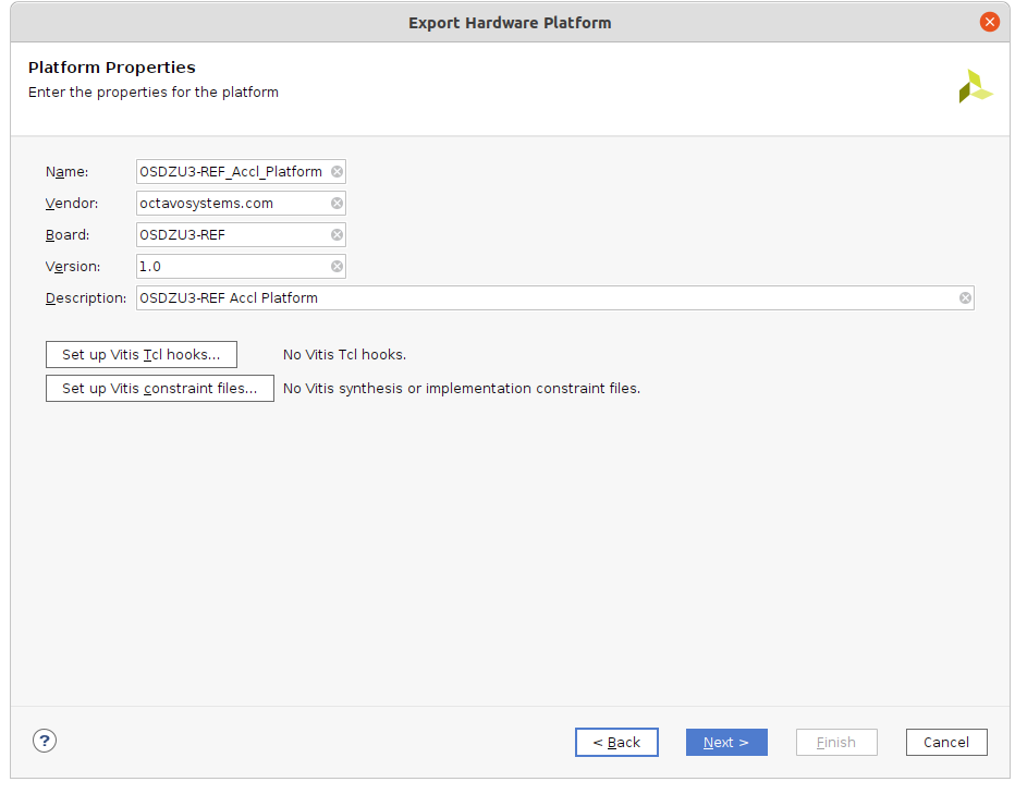

- Fill in XSA file name of your choice
- Click finish. The Acceleration Ready hardware platform will now be exported in the form of a .xsa file. The .xsa file can be imported into a Petalinux project or Vitis as we move forward with our Acceleration Design Flow.

Further Reading
Continue the OSDZU3 Acceleration journey and generate a Petalinux image with Vitis-AI 2.0 and Xilinx Real Time (XRT) support by reading Part 2 of the 4-part Acceleration Tutorial series.
Revision History
Get notified of updates to this Application Note and all of our Technical Documentation.
"*" indicates required fields
| Revision Number | Revision Date | Changes | Author |
| 1 | 11/13/2023 | Initial Revision | Eshtaartha Basu |