How do I design the oscillator circuit for OSD335x family of devices?
The oscillator circuit for real time and system clock inputs is shown in figure 6-9 and 6-12 in the AM335x datasheet.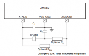
The values of components C1 and C2 referred in the figures depend on the load capacitance (CL) specified by the crystal manufacturer. Load capacitance is calculated as
CL = C1*C2/(C1+C2) + C shunt +C pkg + C pcb
where C shunt is the crystal shunt capacitance also specified by the crystal manufacturer, C pkg and C pcb are the capacitances added due to the interconnections and PCB traces of the design. C pkg and C pcb can be rounded down to 0 -3 pF if the crystal is placed close to the OSD335x and traces are thick enough.
As an example for the 24MHz clock input, let us assume that 7A-24.000MAAJ-T (datasheet) is being used to generate the 24MHz clock signal for OSD335x. The load capacitance on the datasheet is listed as 18pF and the shunt capacitance is listed as 5pF. If we assume C1 and C2 are of equal capacitance and Cpkg + Cpcb are 3pF, C1 and C2 calculated from the above formula come out to be 20pF each.
Similarly for the 32.768Khz clock input, let us assume that ABS07-32.768KHZ-T (datasheet) is being used to generate the 32.768KHz real-time clock. The load capacitance and shunt capacitance on this crystal are listed as 12.5pF and 1.5pF respectively. If we assume C1 and C2 are of equal capacitance and Cpkg + Cpcb are 3pF, C1 and C2 calculated from the above formula come out to be 16pF each.
