Enabling IoT with OSD335x using Wi-Fi and Bluetooth
Published On: March, 13, 2018 By: Neeraj Dantu | Updated: July 18, 2018 by Cathleen Wicks
Wi-Fi is a set of wireless communication technologies developed in the 1990s and 2000s that enables millions of devices to be connected together wirelessly. This has enabled the “Internet-of-Things” (IoT) era in which any device can now be connected to the Internet. Many IoT devices use Wi-Fi to implement a Wireless Local Area Network (WLAN) meeting the IEEE 802.11 standard specifications for Media Access Control (MAC) and Physical Layer (PHY). This article will discuss adding Wi-Fi to the OSD335x Family of System-in-Package (SiP) devices, enabling designers and developers to quickly and easily add IoT functionality to their product.
Table of Contents
1.Introduction
2.Revision History of this Document
3. Adding Wi-Fi to OSD335x
4. WL1835MOD Wireless Module
5. Interfacing WL1835MOD with OSD335x Family
5.1 Power
5.2 Clock
5.3 Interfaces
5.4 Interfacing with OSD335x-BAS
5.5 Layout with OSD335x-BAS
5.5.1 Powering the WL1835MOD
5.5.2 Noise / Thermal design
5.5.3 NRF antenna and SDIO / UART Interface Routing
5.6 Moving from OSD335x-BAS to OSD335x-SM
5.7 Interfacing with OSD335x-SM
5.8 Layout with the OSD335x-SM
5.8.1 Powering the WL1835
5.8.2 Noise / Thermal design
5.8.3 RF antenna and SDIO/UART Interface Routing
6. Software
7. Conclusion
![]()
![]() A PDF version of this App Note can be found here.
A PDF version of this App Note can be found here.
2 Revision History
| Revision Number | Revision Date | Changes | Author |
|---|---|---|---|
| 1 | 3/7/2018 | Initial Release | N. Dantu |

3 Adding Wi-Fi to OSD335x
There are several ways you can add wireless connectivity using the OSD335x Family of SiP devices. The most common way is to add a pre-certified wireless module to the design. Just as the OSD335x Family integrates key components of the system, wireless modules not only integrate all the circuitry required to implement a wireless protocol, but also come pre-certified for commercial use which can ease the regulatory testing requirements on a product. Choosing a wireless module depends largely on the requirements of the product. In this application note, we will look at how to integrate the Texas Instruments WL1835 wireless module with WiLink™ 8 Wi-Fi, Bluetooth and Bluetooth Low Energy (BLE) combo module, WL1835MOD with the OSD335x SiP Family of devices to add wireless capabilities to a product.
4 WL1835MOD Wireless Module
The WL1835MOD wireless module integrates the Radio Frequency (RF) circuitry, power amplifiers, clock, filters, power management and passive components required to implement a wireless networking communication protocol. The RF transceiver operates at 2.4GHz and supports IEEE standards 802.11b, 802.11g and 802.11n, as well as the Bluetooth and BLE protocols. The module uses a 4-bit SDIO interface to communicate to a host for Wi-Fi and a UART interface to communicate to a host for Bluetooth/BLE. A functional block diagram of WL1835MOD taken from the datasheet is shown below:
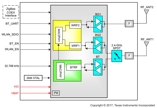
The figure shows that the WL1835MOD module requires two power inputs, VIO and VBAT, and a 32KHz oscillator. It is connected to the host processor through the BT_UART and WLAN_SDIO interfaces. It also has 2 antenna outputs to support the 2×2 MIMO (Multiple-Input-Multiple-Output) functionality of 802.11n.
5 Interfacing WL1835MOD with OSD335x Family
The following figure shows a high-level system diagram showing interfacing between the WL1835MOD module and a host processor running Linux/Android

5.1 Power
WL1835MOD module has 2 power inputs. VBAT_IN is the main 3.3V power supply input and VIO_IN is the 1.8V IO input. The datasheet for the module indicates that the current consumption for the module can go as high as 850mA during calibration, and typically consumes 238 mA while transmitting and 65mA while receiving data. Therefore, it is important to budget for the module power needs accordingly. Since the calibration routine for the module is short, power only needs to be budgeted for the typical current and sufficient bulk capacitors should be added on the input voltage lines to supply the calibration current.
5.2 Clock
A 32KHz external clock is required for the wireless module. A crystal can be used to generate this clock.
5.3 Interfaces
The wireless module has a 4-bit SDIO interface for Wi-Fi and a UART interface for Bluetooth/BLE along with enable signals that can be controlled by the host processor.
The easiest way to add wireless to an application using the OSD335x Family would be to use the OSD335x-SM with the WL1835MOD module. With its small size and increased flexibility, the OSD335x-SM provides and easy path to a wireless enabled application. Please jump ahead to section ‘Interfacing with OSD335x-SM’ if you are using the OSD335x-SM device.
5.4 Interfacing with OSD335x-BAS
The OSD335x-BAS is a 27 mm x 27 mm 400 ball BGA System-in-Package device based on the Texas Instruments AM335x processor. The BeagleBone Black Wireless and BeagleBone Blue provide example implementations of connecting the OSD335x-BAS to the WL1835MOD module.
While BeagleBone Blue uses the OSD335x-BAS SYS_VDD1_3P3V and SYS_VDD_1P8V voltage rails to supply power to the WL1835MOD module, BeagleBone Black Wireless takes a more conservative approach. Both of these approaches will be discussed in this section.
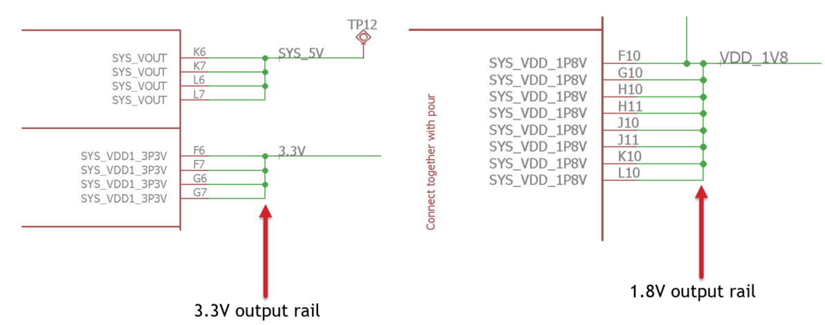
In BeagleBone Blue, both the power input voltages VBAT_IN (3.3V) and VIO_IN (1.8V) are supplied by the OSD335x-BAS external power supply voltage rails, SYS_VDD1_3P3V and SYS_VDD_1P8V, respectively. The following figure shows the schematic diagram of the 3.3V and 1.8V supply voltage connections.
The SYS_VDD1_3P3V can supply 500mA and SYS_VDD_1P8V can provide 250mA. A capacitance of approximately 20uF on the VBAT_IN voltage rail is enough to supply the increased current consumption during the short calibration period.
In designs where the SYS_VDD1_3P3V and SYS_VDD_1P8V voltage rails are being used to power other components on the board, external regulators are needed to power the WL1835MOD. BeagleBone Black Wireless provides a good example of this. The following figure shows the circuit that is used to generate VBAT_IN (3.3V) and VIO_IN (1.8V) for the WL1835MOD:
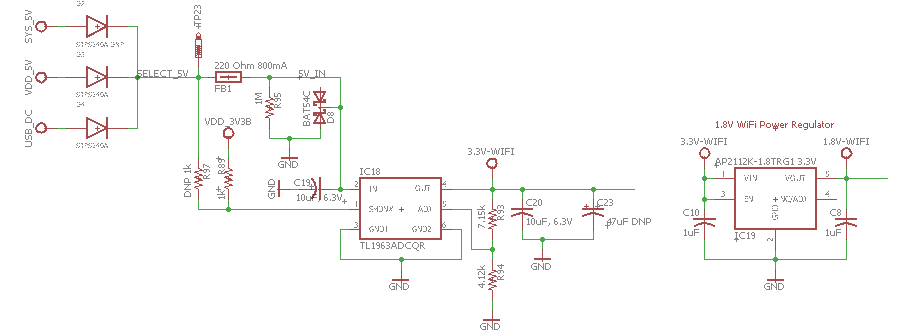
The diodes D2, D3 and D4 multiplex the input to the low-dropout regulator TL1963A so that the LDO gets input power when the board gets powered through different power sources. This is similar to the power muxing that occurs within the TPS65217 power management IC within the OSD335x-BAS. Additional noise filtering and protection circuits are added to the input of the LDO. The LDO is capable of supplying a total of 1.5A output current, which reduces the need for capacitors to supply the calibration current. The resistors R93 and R94 are used to set the output voltage of the LDO to 3.3V. This 3.3V output is in turn used to generate the 1.8V power input needed by the module via a AP2112 fixed voltage LDO.
The WL1835MOD module connections are shown below in the case that external LDOs are used:

The difference between BeagleBone Blue and BeagleBone Black Wireless is the additional capacitance on the 3.3V VBAT_IN voltage rail to supply the calibration current.
Looking at the components and connections around the WL1835MOD, first each line of the UART and SDIO interfaces have termination resistors to mitigate noise. Next, bypass capacitors are used to provide return current paths and noise filtering. Both antennas are connected to coaxial antenna connectors and filtered through 10pF capacitors. Additional noise filtering schemes can be used based on antenna requirements. Finally, a 1.8V power input crystal oscillator (OSC2) is used to supply the module with the required 32.768KHz clock input.
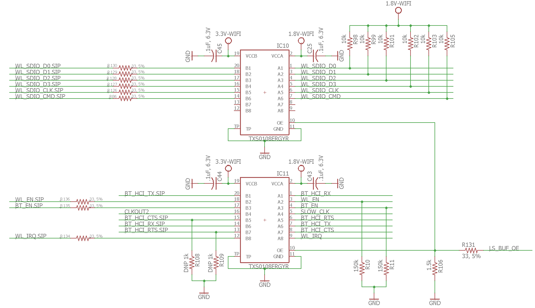
The UART and SDIO interface signals of the WL1835MOD module are 1.8V digital IO signals. Given that all the OSD335x-BAS IOs are 3.3V, level shifters, like the TXS0108E, are required on the signals to interface with the WL1835MOD module. The level shifting circuit is shown below. From the circuit, IC10 translates the 3.3V SDIO signals from the OSD335x-BAS to 1.8V SDIO signals for the module. Similarly, IC11 translates the UART interface, enables and interrupt signals.
The final piece is connecting the UART and SDIO interface signals to the OSD335x-BAS, which is shown in the figure below. Given that in many cases the WL1835MOD module is replacing Ethernet for connectivity, the WL1835MOD module can use the multiplexed functionality of the Ethernet pins to connect to the OSD335x-BAS. For example, the SDIO interface can use the MMC2 peripheral (mode 6 of the Ethernet pins). Similarly, the UART interface can use the UART3 peripheral by selecting mode 1 of the pins and the enables and interrupts can use the GPIO peripheral on mode 7.

5.5 Layout with OSD335x-BAS
Even though the WL1835MOD module is pre-certified to comply with FCC / CE regulations, the layout of the WL1835MOD module is still very important so the board does not emit additional electromagnetic noise or has poor wireless performance. There are three aspects that need attention during routing. They are powering the module, noise / thermal design, and RF trace and antenna routing.
5.5.1 Powering the WL1835MOD:
As discussed in the schematic design, BeagleBone Blue uses the output voltage rails of the OSD335x-BAS to power the WL1835MOD module. The following figure shows the power layout of the WL1835MOD module on BeagleBone Blue. The 3.3V power input to the WL1835MOD is supplied by the SYS_VDD1_3P3V power plane of the board. The 1.8V power input to the WL1835MOD is supplied from the SYS_VDD_1P8V power output of the OSD335x-BAS. Those same voltage rails are also routed to the level shifters for proper voltage translation of the IO signals.

However, in BeagleBone Black Wireless, the WL1835MOD module and the level shifters are powered from external LDOs generating 3.3V and 1.8V. The power layout for the BeagleBone Black Wireless is discussed below:
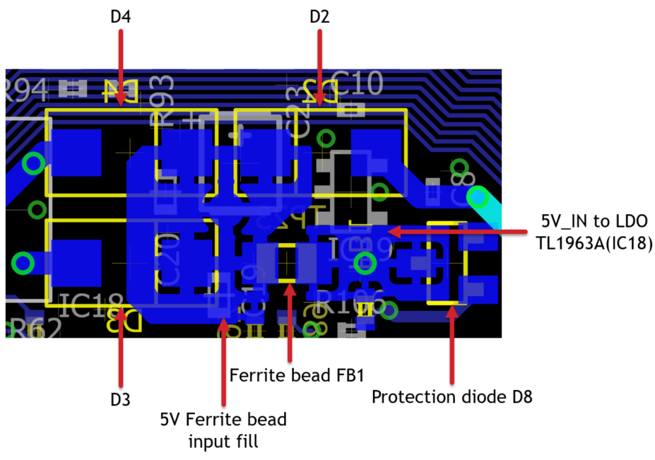
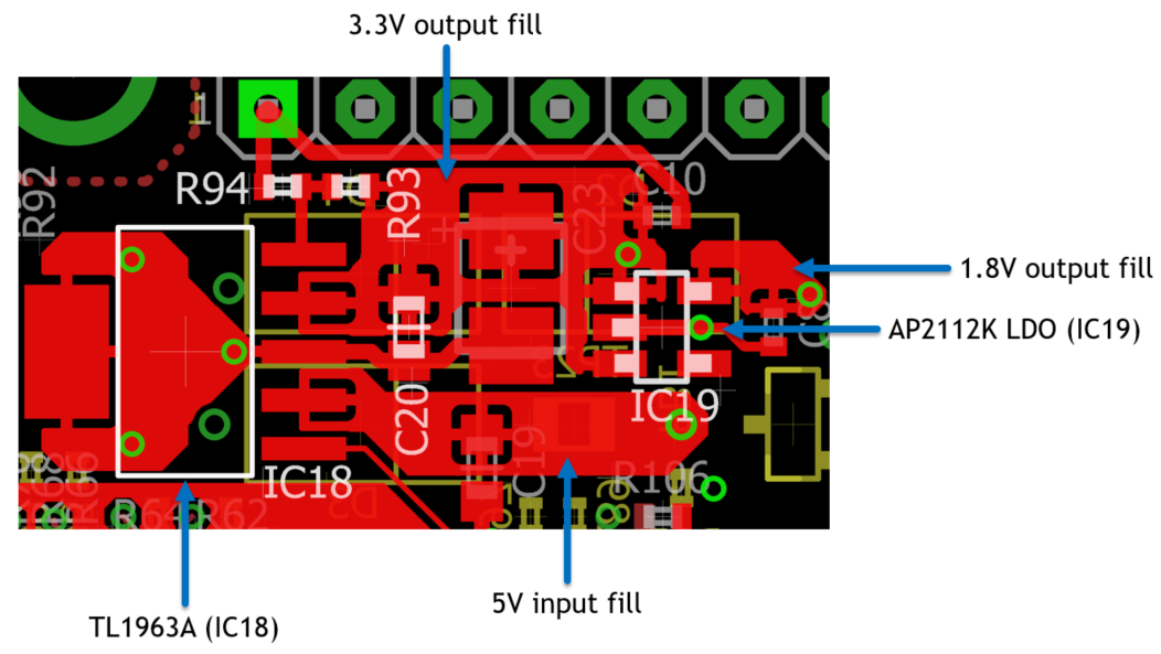
The above figure shows the layout for power input of the LDO TL1963A, which is responsible for powering the WL1835MOD module. Each power rail input for diodes D2, D3 and D4 is a 32-mil width trace. Between the diode outputs and noise cancelling ferrite bead FB1, a copper pour is used to provide maximum connectivity and good thermal performance. Another copper pour is used to connect the output of the Ferrite bead FB1 to the protection circuitry. Given that it is important to have good power flow and thermal performance around the LDOs, copper pours are used for both the 5V input to the TL1963A LDO as well as the 3.3V output which is connected to the LDO AP2112K as seen in the figure below.
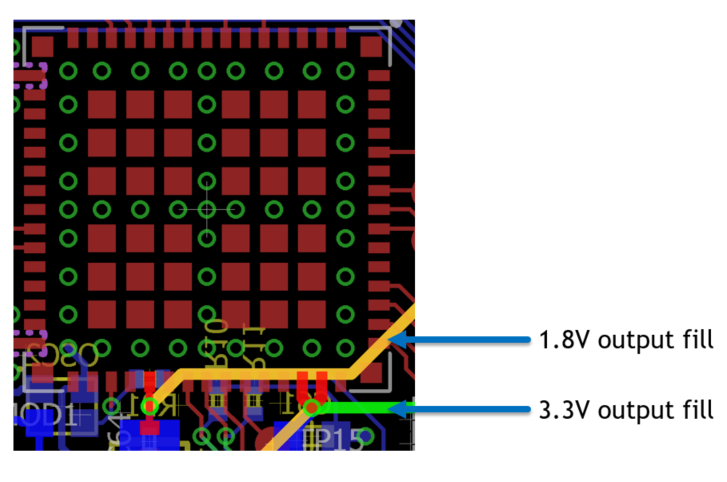
Finally, the output power from the LDOs need to be connected to the wireless module, which is shown in the figure below.
5.5.2 Noise / Thermal design:
There are 36 ground pads under the wireless module. These are needed for a good connection to the ground plane of the printed circuit board to mitigate noise and thermal issues. The following figure shows how a copper pour and a set of vias can form a good connection to the ground plane. In addition to a ground plane underneath the wireless module, a minimal number of signals should be routed underneath the module. This ensures a stable system with minimal noise and good thermal dissipation.

5.5.3 RF antenna and SDIO / UART Interface Routing:
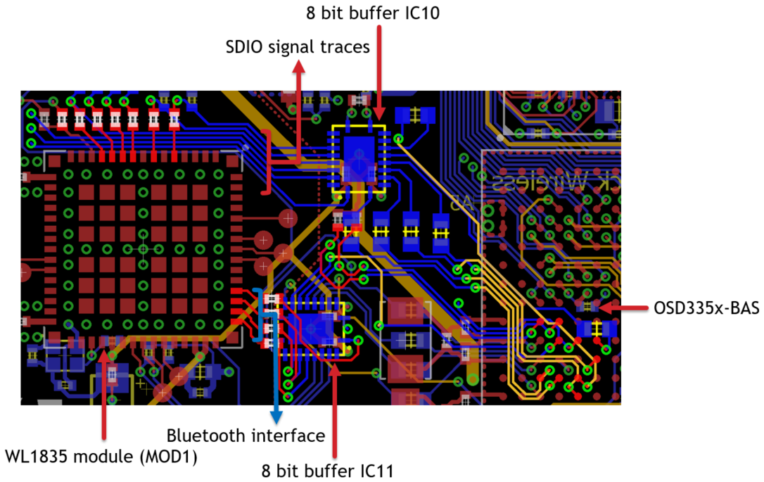
The above image shows the SDIO and UART interface signal routing between the OSD335x-BAS and the WL1835MOD module. As described in the schematic section, two (2) 8-bit level shifters are used to translate the voltages of the IO signals between the OSD335x and the WL1835MOD. Given the speed of the SDIO interface, it is recommended that the routes for the SDIO signals, CLK, CMD, D0, D1, D2 and D3, are under 12cm and are length matched. Ideally, the spacing between the SDIO traces should be 1.5 times the trace width, which is set to 6-mil.
The traces that feed the RF antenna connector from the WL1835MOD have signals running at 2.4GHz. Therefore, they are routed with great care to ensure good RF performance. The placement of the module is such that the antenna traces are at the edge of the PCB. Also, the RF traces are as short as possible with appropriate ground reference underneath the routing layer. Via stitching around the RF trace between the copper pour of ground on the top layer of the printed circuit board and the ground plane is done to minimize noise. The RF traces should have gradual bend with mitered traces, versus any type of sharp corner. The maximum bend allowed on these traces is 90 degrees. These traces also need to have constant impedance. The RF antenna feed trace routing in BeagleBone Black Wireless is shown highlighted below:
5.6 Moving from OSD335x-BAS to OSD335x-SM
There are only two main differences between interfacing the WL1835MOD module with the OSD335x-BAS and the OSD335x-SM device.
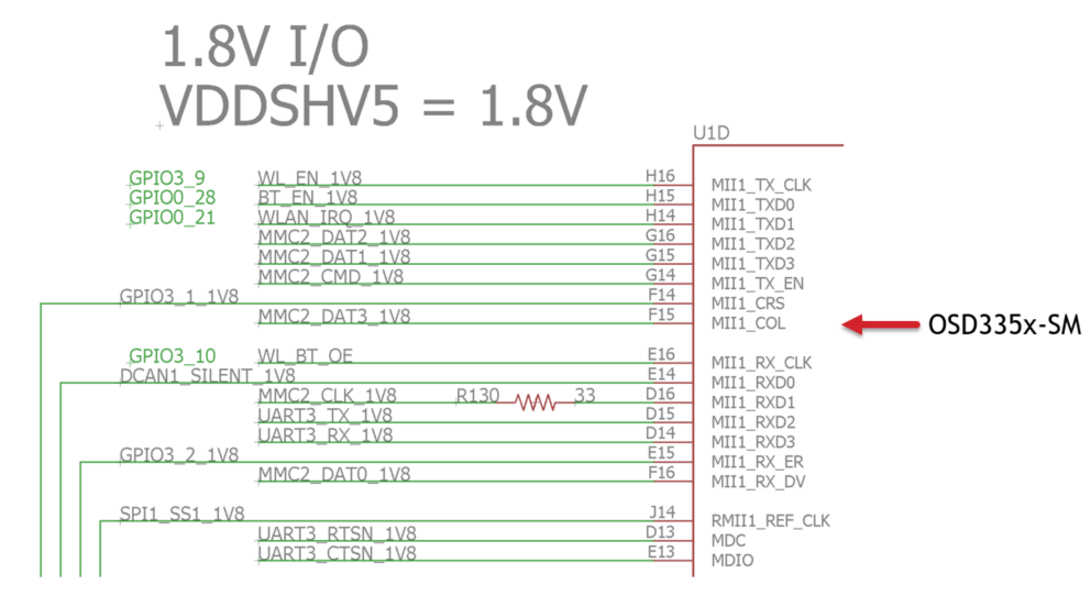
The first difference is that the SDIO and UART interface pin group of OSD335x-SM can be set to 1.8V level logic by driving the VDDSHV5 pin with 1.8V. This will allow for the SDIO and UART interfaces of the wireless module to be connected to the OSD335x-SM directly instead of going through level shifters. This is shown in the schematic below:
The second difference is that the pin-out of the OSD335x-SM is different from the OSD335x-BAS. The OSD335x-SM is a 256 pin 21 mm x 21 mm BGA device. The pin assignment mapping for both OSD335x-BAS and OSD335x-SM with the AM335x can be found here: https://octavosystems.com/app_notes/osd335x-family-pin-assignments/
5.7 Interfacing with OSD335x-SM
The OSD335x-SM is a 21mm x 21mm, 256 BGA package System in Package based on the AM335x processor. Because of added flexibility, it is the easier device to interface with the WL1835MOD module.
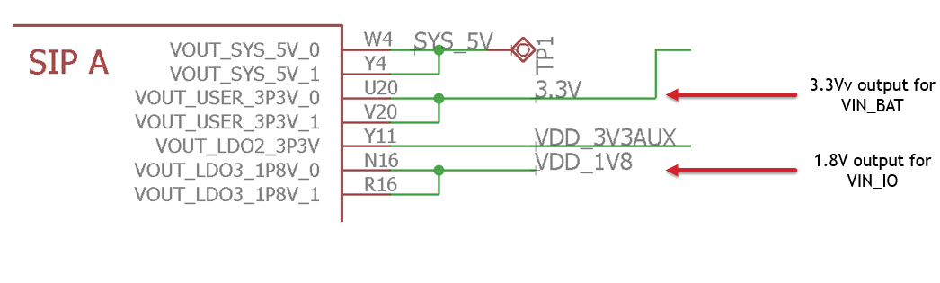
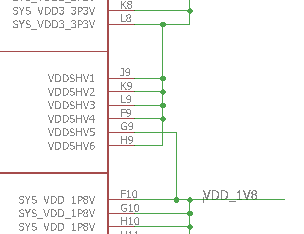
The power input of WL1835MOD, VBAT_IN(3.3V) and VIO_IN(1.8V) can be drawn from the OSD335x-SM external power supply voltage rails, SYS_VDD1_3P3V and SYS_VDD_1P8V respectively. The following figure shows the schematic diagram of the supply voltages 3.3V and 1.8V being drawn from the OSD335x-SM.
The SYS_VDD1_3P3V voltage rail can supply 500mA and SYS_VDD_1P8V voltage rail can provide 250mA. A capacitance of approximately 20uF on the VBAT_IN voltage rail is enough to supply the instantaneous spikes in current consumption during the short calibration period.
In designs where SYS_VDD1_3P3V and SYS_VDD_1P8V are being used to other components on the board external regulators are needed to power WL1835 as described in the ‘Interfacing with OSD335x-BAS’ section. The WL1835MOD module circuit schematic is shown below:
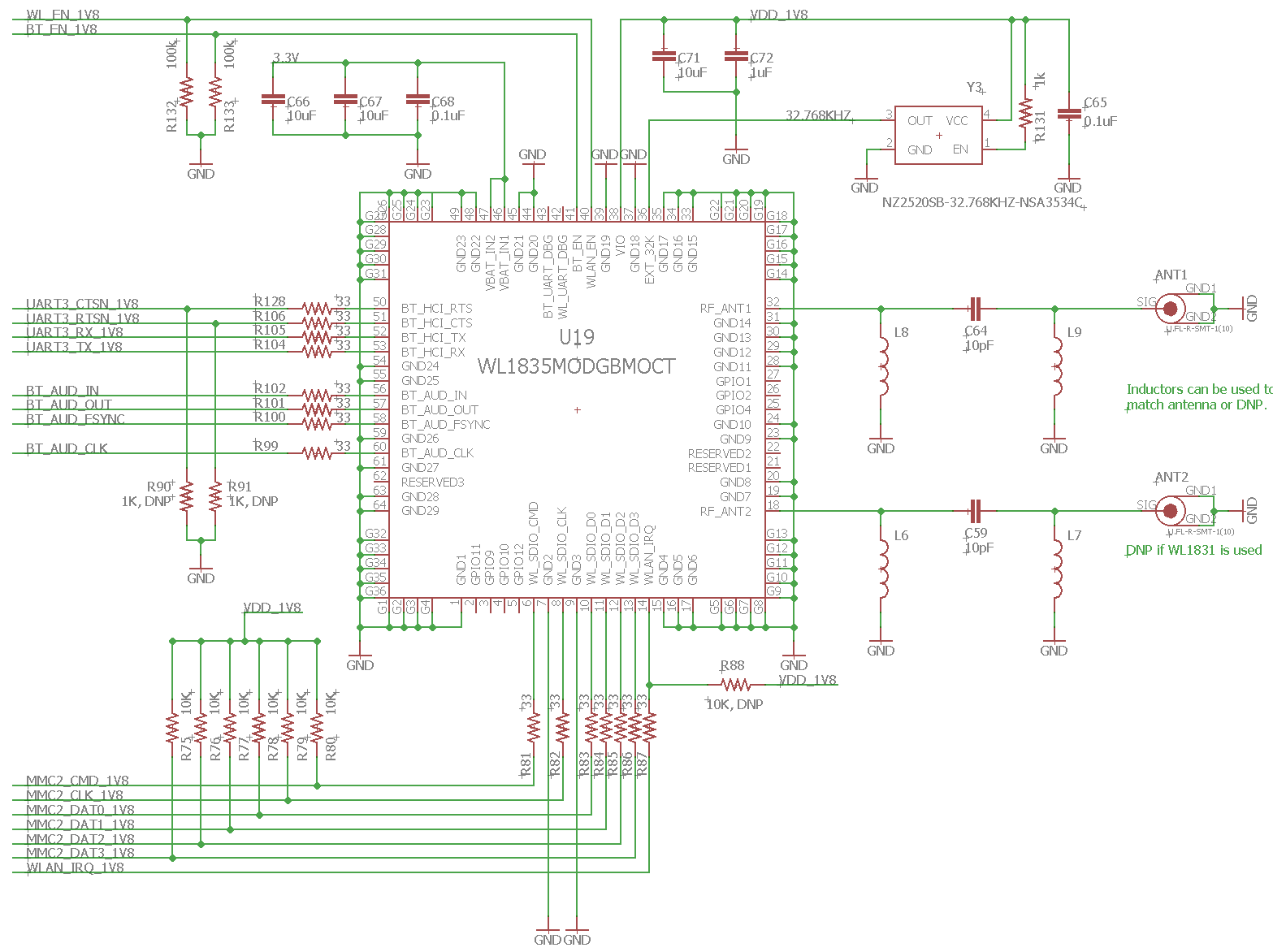
Looking at the components and connections around WL1835, first each line of the Bluetooth (UART3) and SDIO (MMC2) interfaces have termination resistors to mitigate noise. Next, bypass capacitors are used to provide return current paths and noise filtering. Both antennas are connected to coaxial antenna connectors and filtered through 10pF capacitors. Additional noise filtering schemes such as inductances in parallel can be used based on antenna requirements. Finally, a 1.8V power input crystal oscillator (Y1) is used to supply the module with the required 32.768KHz clock input.
The following figure shows the Wi-Fi(MMC2) and Bluetooth(UART3) signals connected to OSD335x-SM.
As shown, the final piece is connecting the UART and SDIO interface signals to the OSD335x-SM. Given that in many cases the WL1835 module is replacing Ethernet for connectivity, the WL1835 module can use the multiplexed functionality of the Ethernet pins to connect to the OSD335x-SM. For example, the SDIO interface can use the MMC2 peripheral (mode 6 of the Ethernet pins). Similarly, the UART interface can use the UART3 peripheral by selecting mode 1 of the pins and the enables and interrupts can use the GPIO peripheral on mode 7.
5.8 Layout with the OSD335x-SM
Even though the WL1835 module is pre-certified to comply with FCC / CE regulations, the layout of the WL1835 module is still very important so the board does not emit additional electromagnetic noise or has poor wireless performance. There are three aspects that need attention during routing. They are powering the module, noise/thermal design, and RF trace and antenna routing.
5.8.1 Powering the WL1835:
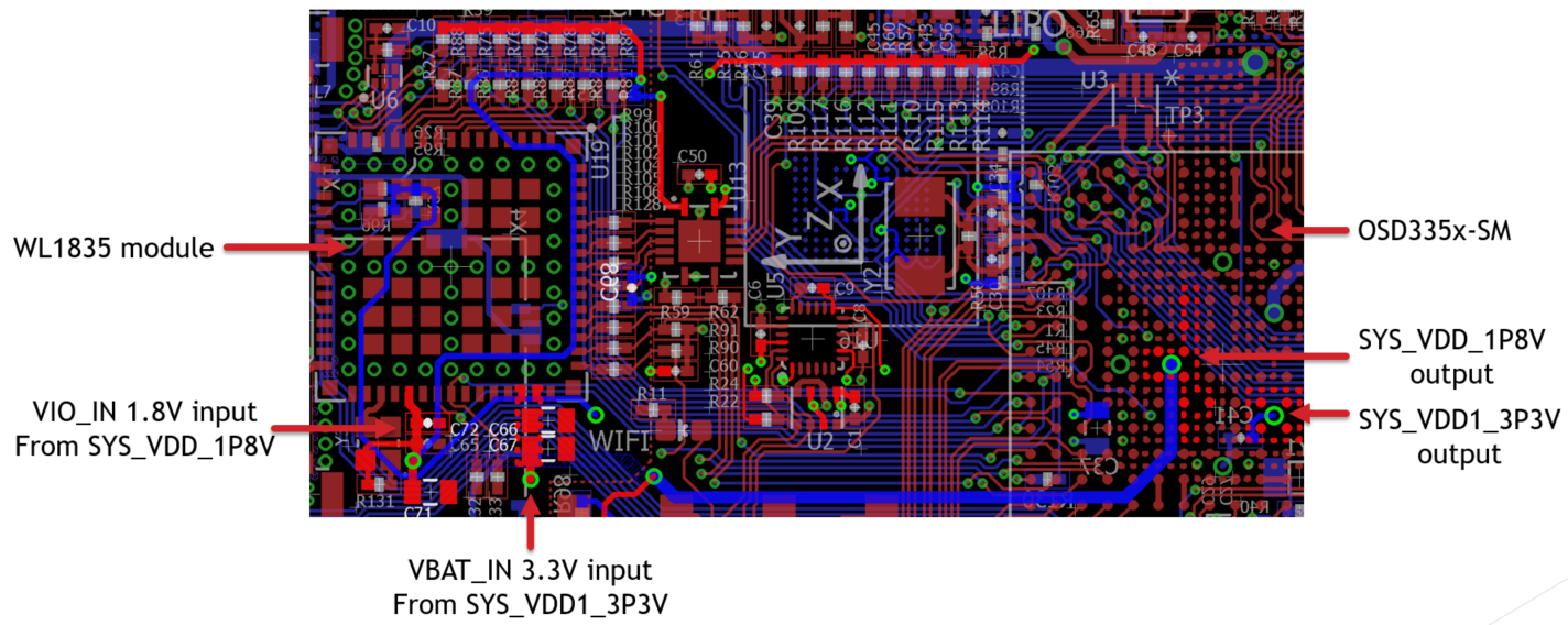
As discussed in the schematic design, the output voltage rails of the OSD335x-SM can be used to power the WL1835MOD module. The following figure shows the power layout of the WL1835MOD module on with the OSD335x-SM. The 3.3V power input to the WL1835 is supplied by the SYS_VDD1_3P3V power plane of the board. The 1.8V power input to the WL1835 is supplied from the SYS_VDD_1P8V power output of the OSD335x-SM. The highlighted power rails are shown below:
5.8.2 Noise / Thermal design:
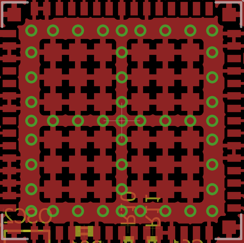
There are 36 ground pads under the wireless module. These are needed for a good connection to the ground plane of the printed circuit board to mitigate noise and thermal issues. The following figure shows how a copper pour and a set of vias can forma good connection to the ground plane. In addition to a ground plane underneath the wireless module, a minimum number of signals are routed underneath the module. This ensures a stable system with minimal noise and good thermal dissipation.
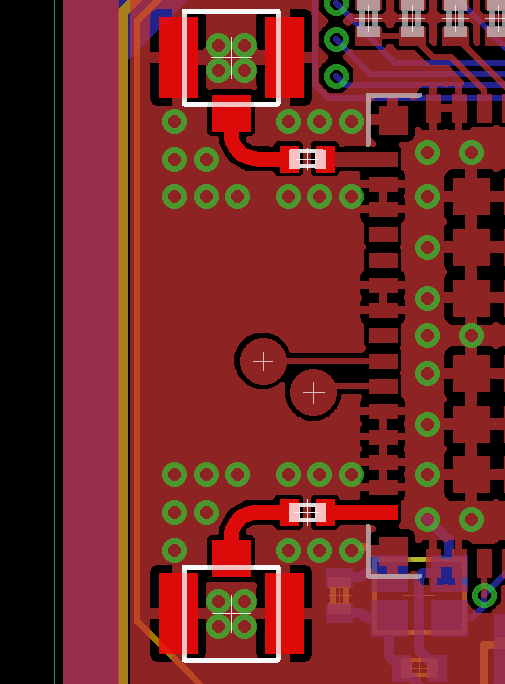
5.8.3 RF antenna and SDIO/UART Interface Routing:
The following image shows the SDIO and UART interface signal routing between the OSD335x-SM and the WL1835MODmodule.
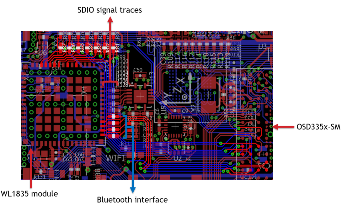
Given the speed of SDIO interface, it is recommended that the traces for SDIO (MMC2) signals CLK, CMD, D0, D1, D2 and D3 are under 12cm and are length matched. Ideally, the spacing between the SDIO traces should be 1.5 times the trace width which is set to 6 mil.
The traces that feed the RF antenna connector from the WL1835 have signals running at 2.4GHz. Therefore, they are routed with great care to ensure good RF performance. The placement of the module is such that the antenna traces are at the edge of the PCB. Also, the RF traces are as short as possible with appropriate ground reference underneath the routing layer. Via stitching around the RF trace between the copper pour of ground on the top layer of the printed circuit board and the ground plane is done to minimize noise. The RF traces have gradual bend with mitered traces, vs any type of sharp corner. The maximum bend allowed on these traces is 90 degrees. These traces also need to have constant impedance. An example of the RF antenna feed trace routing is shown highlighted below:
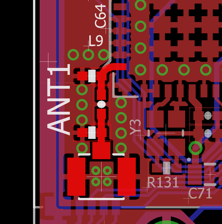
The figure also shows an example of filtering elements (capacitors and inductors) placed in series/parallel to the trace aligning the pads along the signal path or perpendicular to it with no edges or deviations along the path.
6 Software
Once the hardware has been connected and properly laid out, there is software needed to configure a board to use the WL1835MOD. Linux needs a special data structure called a device tree to understand the peripherals connected to the processor. This application note assumes use of Beagleboard.org images for software development.
A good resource to get started on the device tree is the device tree rebuilder (https://github.com/RobertCNelson/dtb-rebuilder). This Git repository contains device tree source files written for different AM335x development boards that can be used as references for a custom board. The device tree source file am335x-boneblack-wireless.dts for the Beaglebone Black Wireless is present in src/arm directory of the repository. The DTS file includes the am335x-boneblack-WL1835MOD.dtsi file to describe which AM335x pins are used to interface with the WL1835MOD module and instruct the kernel which drivers are required to communicate with the WL1835MOD module.
After compiling the new device tree binary file using the device tree rebuilder, the device tree binary file needs to be placed in /boot/dtbs/[Kernel version]/ in order for the kernel to find the new device tree. After doing this, the custom device tree name needs to be specified as a boot environment variable ‘dtb’ in the /boot/uEnv.txt file.
To summarize, here is the procedure to boot a custom wireless board with WL1835MOD module and OSD335x family of SiPs:
- Use the BeagleBone Black Wireless/ BeagleBone Blue device trees as a reference to build a custom device tree
- Compile the device tree suing device tree rebuilder
- Copy the device tree binary file into /boot/dtbs/[Kernel version]/
- Set dtb boot variable to custom device tree binary name in /boot/uEnv.txt
This should allow the board to boot and have full wireless capability.
7 Conclusion
This application note describes the hardware and software steps to integrate the WL1835MOD wireless module with the OSD335x family to provide wireless capabilities and enabling IoT functionality. For more information, please refer to the following links:
- Datasheet for WL18xxMOD WiLink™ 8 Single-Band Combo Module –Wi-Fi®, Bluetooth®, and Bluetooth® Low Energy (LE) (SWRS152M) http://www.ti.com/lit/ds/symlink/wl1805mod.pdf
- OSD335x-BAS datasheet: https://octavosystems.com/docs/osd335x-datasheet/
- OSD335x-SM datasheet: https://octavosystems.com/docs/osd335x-sm-datasheet/
- Device tree rebuilder: https://github.com/RobertCNelson/dtb-rebuilder
- BeagleBone Black Wireless: https://beagleboard.org/black-wireless
- BeagleBone Blue: https://beagleboard.org/blue
