
The Future of SiP: Providing a BreadBoard in a Tiny Package
As Moore’s Law approaches retirement age[1][2], the technological advances wrought through the improvements in silicon process technology are staggering. The ability to tailor a process for high power, high voltage power electronics vs low power, low voltage, extremely dense microprocessor and memories enables the proliferation of technology in the age of the Internet of Things (IoT). However, for all the advancements, each silicon component can only have one process; a compromise necessary for each circuit that needs to be optimally built. Where Moore’s Law left off from the perspective of the individual component, packaging technology has taken up the reigns. Packaging technologies are able push the boundaries of form, fit, and function beyond that which is possible with System on a Chip (SoC) technology. Systems in a Package (“SiP”s) can enable new levels of integration and size reduction for embedded systems[3][4]. However, like the technologies that have come before it, SiPs require enormous investments of design time and effort. In this paper, we introduce the future of SiP: the Universal Connection Matrix (UCM) . This allows for faster design and prototyping with SiP devices. Instead of large, monolithic designs, the UCM provides a breadboard in a package.
SiPs Provide Heterogeneous Integration
In the silicon industry, single fixed-function Application Specific Integrated Circuits (ASICs) have given way to System-on-a-Chip (SoC) devices for most embedded system applications. SoCs incorporate many different functional circuit blocks, including both analog and digital circuits, on a single monolithic block of silicon to form one piece of an embedded system. Similarly, a chip package has historically been a single fixed-function device to provide access to the silicon device inside. However, with the development of advanced packaging techniques, SiP devices are now able to integrate multiple silicon devices alongside packaged devices and passive components on a single package substrate. This means that the package substrate has become a miniature printed circuit board (PCB). SiPs enable all components of an embedded system, such as digital devices, analog circuits, memories, sensors, power management, and wireless devices to be integrated together into a single component. These components can have diverse fabrication technologies and might otherwise be impossible or impractical to integrate together into a single block of silicon. However, similar to SoCs, there is an up-front design cost to develop the SiP substrate, which can impact time to market, as well as the limitation of each substrate design having a fixed functionality.
Universal Connection Matrix (UCM) : Flexibility for Designers
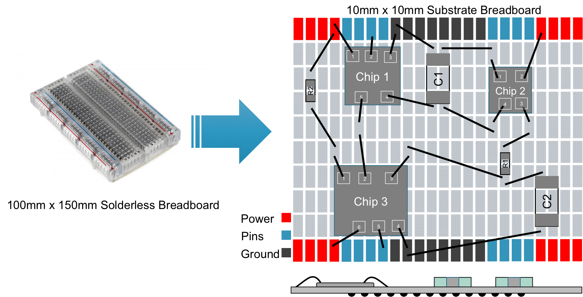
To avoid the fixed nature of SiP devices and improve the ability to prototype using SiP technology, we propose the Universal Connection Matrix. The UCM is a matrix of connection pads covering all or a portion of the package substrate. These pads are generic connection pads. Discrete components, such as resistors, capacitors, bare die and packaged devices, can be placed on top of the pads similar to how components are mounted to footprint pads on a printed circuit board (PCB). The components are electrically connected to the pads either through solder, similar to surface mount components, or in the case of bare die with bond wires from the bond pads to the UCM pads. Once all the components are mounted, they are then electrically connected together using bond wires between the UCM pads. The bond wires form an interconnect to complete the desired circuit and allow all of the components to function together. Similar to a breadboard, the UCM provides the foundation that allows the components within the SiP device to be connected together.
The generic nature of the UCM allows a single SiP substrate to be used for multiple designs. This allows many, low volume products to be manufactured quickly using the same substrate on the same production line by only changing the placed components and bond wire interconnect. This reduces manufacturing cycle time to create a packaged device from eight to twelve weeks to approximately two weeks. The cycle time reduction is primarily due to the fact that substrates do not have to be manufactured for each new device. Instead, new devices can be created by just re-programming the wire bonder and pick-and-place machine. This capability opens a new integration path to low volume applications.
Beyond using UCM technology for low volume applications, it can be used extensively where rapid prototyping is required. In the same way that FPGA allows designers to prototype logic circuit designs that can later be optimized into an ASIC or SoC, the UCM allows designers to prototype embedded system designs that can later be optimized into a SiP. Also, in the same way that FPGAs consume more silicon area in order to provide design flexibility, the UCM consumes more package substrate area than an optimized SiP design. To minimize area and cost while still maintaining flexibility, a SiP does not need to be entirely composed of a UCM. There are certain components in an embedded system that are common to many application spaces, for example a microprocessor, memory, and power management. A SiP can be designed such that common components have a fixed implementation and a portion of the substrate contains a UCM. Similar to newer hybrid FPGAs, this heterogenous methodology allows designs to leverage the density of advanced SiP technology while still maintaining the flexibility that the UCM affords.
Giving Small Customers Access to Advanced Technology
As SiP technology proliferates to more and more packaged devices, the ability to easily and efficiently create differentiated designs quickly becomes paramount. The UCM and associated design tools simplify the design process and allows for rapid development of small form factor SiP designs. As designers once used breadboards to design the next great product idea, in the future, they will use the UCM.
***
Co-authored by Gene Frantz and Masood Murtuza, This paper was presented at the 2018 International Microelectronics Assembly and Packaging Society Symposium. The full paper content will be available for download from the iMAPs Society. Please contact us if you would like to keep up with what we are doing to advance the state of the art of SiP technology. We look forward to hearing from you!
You can also sign up for our mailing list or follow us on Facebook, Twitter, or Linked In.
References:
[1] Moore, Gordon. “Cramming more components onto integrated circuits” Electronics, Volume 38, Number 8, 19 April, 1965. [2] Loughran, Jack. “Moore’s Law 2017: an uphill battle” Engineering & Technology, The Institution of Engineering and Technology, 19 May 2017, [3] Deo, Manish. “Enabling Next-Generation Platforms Using Intel’s 3D System-in-Package Technology” Altera Inc., 16 Dec. 2017, [4] ITRS. “ITRS Assembly and Packaging 2007 Roadmap” International Electronics Manufacturing Initiative, 2007,