Tag: OSD335x
The OSD335x family supports all the frequencies supported by corresponding AM335x present inside. For example, the AM3358 inside the OSD3358 supports 6 Operational Performance Points(OPP). It can run at 300MHz, 600MHz, 720MHz, 800Mhz and 1GHz. These operational performance points are set using the Digital Phase Locked Loops(DPLLs) and MPU, CORE voltages on the AM335x. The following figure from the AM335x datasheet (Table 5-7) shows the OPPs, the corresponding MPU voltage to be set and the frequency of operation of the OPP (Source: AM335x datasheet).
| VDD_MPU OPP | VDD_MPU | ARM Clock Speed | ||
|---|---|---|---|---|
| MIN | NOM | MAX | ||
| Nitro | 1.272 V | 1.325 V | 1.378 V | 1 GHz |
| Turbo | 1.210 V | 1.260 V | 1.326 V | 800 MHz |
| OPP120 | 1.152 V | 1.200 V | 1.248 V | 720 MHz |
| OPP100 | 1.056 V | 1.100 V | 1.144 V | 600 MHz |
| OPP50 | 0.912 V | 0.950 V | 0.988 V | 300 MHz |
The oscillator circuit for real time and system clock inputs is shown in figure 6-9 and 6-12 in the AM335x datasheet.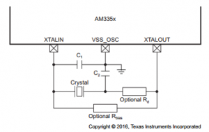
The values of components C1 and C2 referred in the figures depend on the load capacitance (CL) specified (more…)
direct linkYes we do. You can find the OSD335x Family Pin Assignments table here.
direct linkThe ball map of the OSD335x-BAS/IND was designed to match the ball map of AM335x ZCZ package except for a few changes. The following figure highlights the changes that were made to AM335x ZCZ ball map.
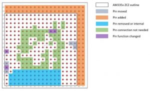
Violet and Grey pins are the only pins that have been moved or functionally changed.
Blue pins (AM335x DDR interface) should be left unconnected.
Green pins (AM335x Power input pins) should be left unconnected or brought out as test points for monitoring.
Orange pins are additional pins added to the package for more functions.
Please refer the datasheet of OSD335x-BAS for their functional description.
The major changes in functionality are listed below. (more…)
direct linkAll the peripherals supported by the AM335x are also supported by the OSD335x-BAS/IND. However, the OSD335x-BAS/IND only supports 3.3V I/Os. Please refer to question ‘What are the differences in ball maps of AM335x and OSD335x?‘ for ball map differences between OSD335x and AM335x.
direct linkNo, you don’t. The AM335x die in the OSD335x is the same as the Die in the discrete TI device. This means that the Pin Mux will work the same on the OSD335x as it would on the discrete version. There are minor differences in location and position of a few signals. Please refer to question ‘What are the differences in ball maps of AM335x and OSD335x?‘ for ball map differences between OSD335x and AM335x.
direct linkThe pins of OSD335x correspond to the ZCZ package of the AM335x.
direct linkThere are 3 use case scenarios for RTC functionality. They are the RTC-only mode which allows all the power supplies except for the RTC to be turned off to save power, RTC timer functionality mode in which the Real Time clocking features are used and RTC disabled mode in which RTC features are not used. Use of RTC requires both software and hardware setups. The hardware requirements of various RTC configurations are shown below and described in detail in the AM335x schematic checklist. Note that RTC-Only mode is not supported by the OSD335x family of devices because of the version of the PMIC (TPS65217C) used to power AM335x.
| Pin | Function | RTC timer functionality but no RTC-only mode | RTC feature disabled |
|---|---|---|---|
| CAP_VDD_RTC | RTC core voltage input | No Connect | VDD_CORE |
| RTC_KALDO_ENn | Internal LDO enable input | Pulled down to VSS | Pulled up to SYS_RTC_1P8V |
| RTC_PWRONRSTn | RTC Power On Reset input | PMIC_OUT_LDO_PGOOD | VSS |
| PMIC_POWER_EN | PMIC power enable output | PMIC_IN_PWR_EN | No Connect |
| EXT_WAKEUP | External wakeup input | PMIC_OUT_NWAKEUP | VSS |
While there are Linux drivers available for the RTC, the following steps describe the low-level software procedure to enable use of an external 32Khz oscillator for RTC clock input.
Begin with writing the KICK registers to disable write protect to RTC registers.
- Write the value 0x83E70B13 to KICK0R (0x44E3E06C) register.
- Write the value 0x95A4F1E0 to KICK1R (0x44E3E070) register.
RTC_OSC_REG (0x44E3E054) register needs to be modified to enable external oscillator clock input. Set RTC_OSC_REG[4] to 1 to select external 32KHz oscillator as clock source and RTC_OSC_REG[6] to enable clock mux of RTC. Note that 0 at RTC_OSC_REG[2] enables the use of internal feedback resistor instead of an external one.
- Write the value 0x48 to RTC_OSC_REG (0x44E3E054).
The procedure can be verified by either probing the output of the 32KHz (OSC1) oscillator or probing the XDMA_EVENT_INTR1 signal selecting OSC1 as its clock source.
direct linkThe AM335x inside of the OSD335x family of devices can directly drive LCD panels. Here is an overview pulled from the AM335x datasheet on TI.com
- LCD Controller
- Up to 24-Bit Data Output; 8 Bits per Pixel (RGB)
- Resolution up to 2048 × 2048 (With Maximum 126-MHz Pixel Clock)
- Integrated LCD Interface Display Driver (LIDD) Controller
- Integrated Raster Controller
- Integrated DMA Engine to Pull Data from the External Frame Buffer Without Burdening the Processor via Interrupts or a Firmware Timer
- 512-Word Deep Internal FIFO
- Supported Display Types:
- Character Displays – Uses LIDD Controller to Program these Displays
- Passive Matrix LCD Displays – Uses LCD Raster Display Controller to Provide Timing and Data for Constant Graphics Refresh to a Passive Display
- Active Matrix LCD Displays – Uses External Frame Buffer Space and the Internal DMA Engine to Drive Streaming Data to the Panel
(Source: AM335x datasheet)
direct linkThe MUX_OUT pin of the PMIC (TPS65217C) can be connected to the ADC channels of the AM335x externally on the OSD335x-SM device. The ball numbers for each of the PMIC_MUX pins and commonly used ADC channel are given below:
| OSD335x-SM Signal Name | Ball Number |
| PMIC_MUX_IN | N13 |
| PMIC_MUX_OUT | D6 |
| AIN7 | D7 |
But, OSD335x (OSD3358-BAS) DOES NOT support this functionality since MUX_IN and MUX_OUT pins are not externally accessible on this device.
direct link