
PocketBone: The Linux Computer that Fits in a Mini-Altoids Tin – Designed in KiCad – Featuring the OSD3358
This article was guest written by Michael Welling, the developer of the KiCad PocketBone Design. Michael is an Embedded Design Engineer with over 10 years of experience. He owns an electronic design consulting firm, QWERTY Embedded Design, LLC. He has an MS in Electrical Engineering, was an instructor at SIUC and a 12-year member of IEEE. He is also a mentor for Beagleboard.org Google Summer of Code.
Motivation
As an embedded systems design engineer, I am always on the lookout for the latest technology. When the Octavo Systems OSD3358 was announced I was very excited to see something mainstream using System-In-Package (SiP) technology.
System-In-Package represents a new way to overcome many design challenges in the highly integrated mixed signal system space. The OSD3358, in particular, piqued my interest because I had done a few designs using the Texas Instruments Sitara® series System on Chips (SoC), the same one at the core of this Octavo SiP. This urged me to design something around the SiP. I really wanted to compare the design process of the SiP to that of a typical SoC.
The benefits of having the DDR memory integrated into the package are obvious to anyone that has done work with typical SoCs with external RAM. DDR memory routing and design rules are quite complex and require a substantial amount of work at design time. From trace equalization to differential pair routing, the DDR routing process usually has the engineer rolling up their sleeves.
The integration of the power supplies and passives removes many of the SoC design challenges. Most SoCs require several power supplies that must be enabled in a very specific and timed sequence. Typically, integrated power management ICs (PMIC) are used to meet these requirements but they still require sourcing of passives, including the appropriately sized inductors for the embedded switching regulators.
As a bonus, the SiP even integrates the bypass capacitors that are typically sprinkled all over the opposite side of the PCB from the SoC. This leaves more area on the bottom of the PCB for placement when doing highly space-constrained designs. With all of this built into the SiP, I knew the design process was going to be a breeze.
So when I was approached to do a community reference design with the SiP, I knew it was time to step forward.
The History of PocketBone
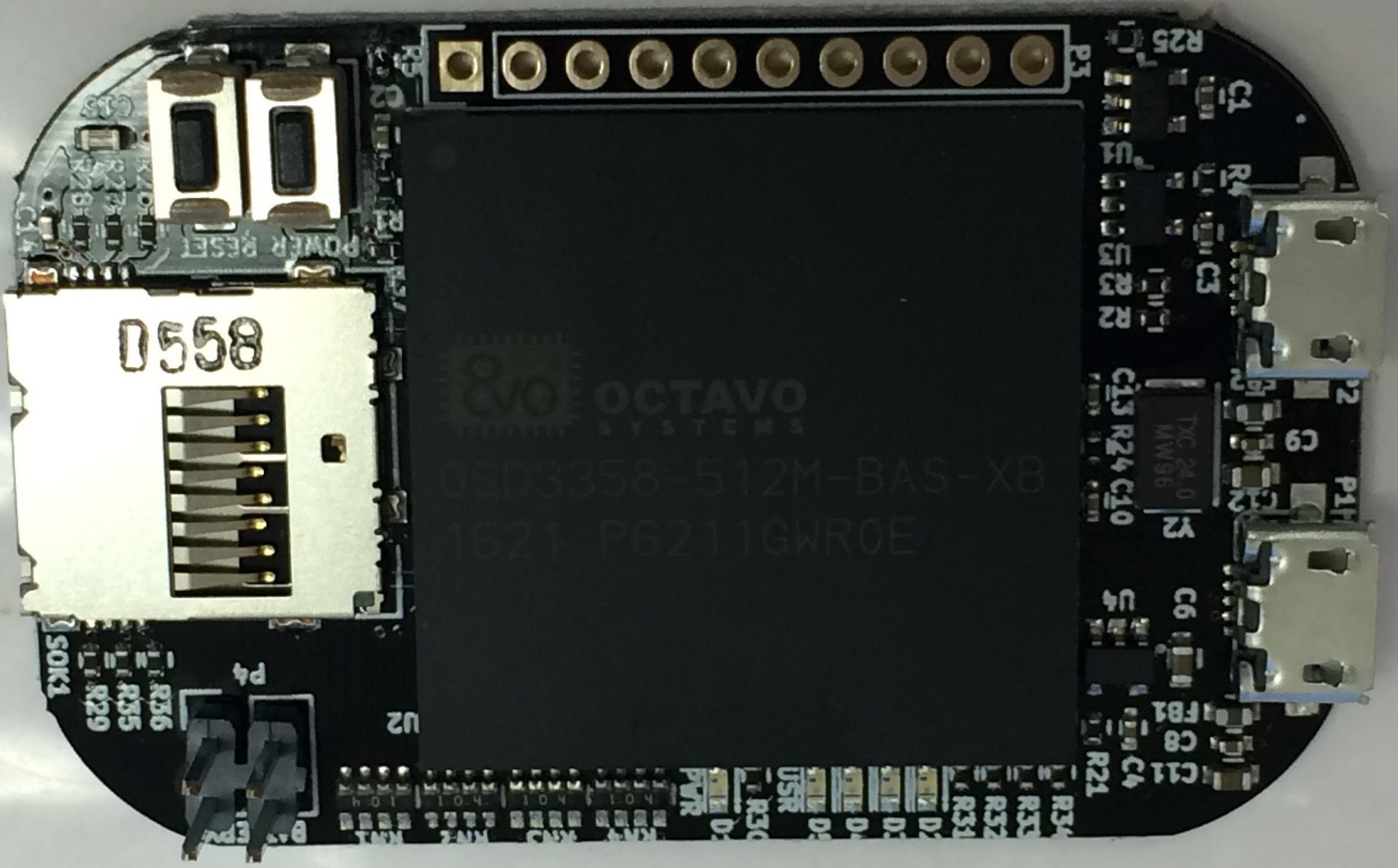
T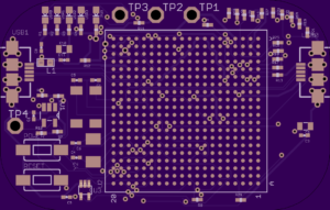 he PocketBone started out as a small reference design in Eagle CAD developed by Jason Kridner of the Beagleboard.org foundation. It was meant to provide a starting point for the community to take and create their own designs. The original board broke out USB, MicroSD, and a few LEDs. The form factor was truly impressive, a Beagleboard in a small Altoids tin.
At the Linux Plumbers Conference, the design was brought to my attention after I expressed interest in doing a design with the Octavo SiP to Drew Fustini. Drew had recently become a board member for Beagleboard.org and said that they were looking to hand off the PocketBone project to someone.
Drew explained the state of the project and the desire to convert the project from Eagle to KiCAD to make the design more accessible to the community. We discussed documenting the design process and the possibility of doing home assembly of the units. Furthermore, the final assembly would be recorded and posted as a reference for aspiring hardware hackers.
Needless to say, I took the challenge and started work soon after returning home from the conference.
The Schematics
The schematic was translated rather quickly from Jason’s design. One thing that accelerated the translation was the existing KiCAD component symbol and footprint provided from a library by Alex Hiam, a fellow Beagleboard.org GSoC mentor.
While pulling the schematic across from Eagle a few errors in the original design were discovered and corrected as necessary. The original design had various issues with the crystals and USB. I also added a 10 pin header which broke out SPI, I2C, and UART0 to add a bit more functionality.
All of the design files were pushed to Github and are publically available at https://github.com/mwelling/pocketbone-kicad
Once I completed the design it was reviewed by some other BeagleBoard.org community members. The design was so simple there really wasn’t much to review and I moved onto routing.
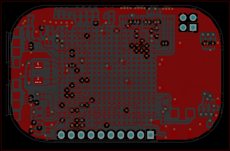
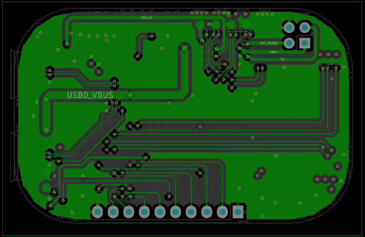
Routing
For the first pass at routing, I attempted using 2 layers to route the design. Though it was possible to route in 2 layers I wasn’t completely satisfied with my attempt. First, I had concerns about routing USB traces in 2 layers and not having the proper impedance. Also, some of the components placements I chose made it difficult to make cases for the PocketBone.
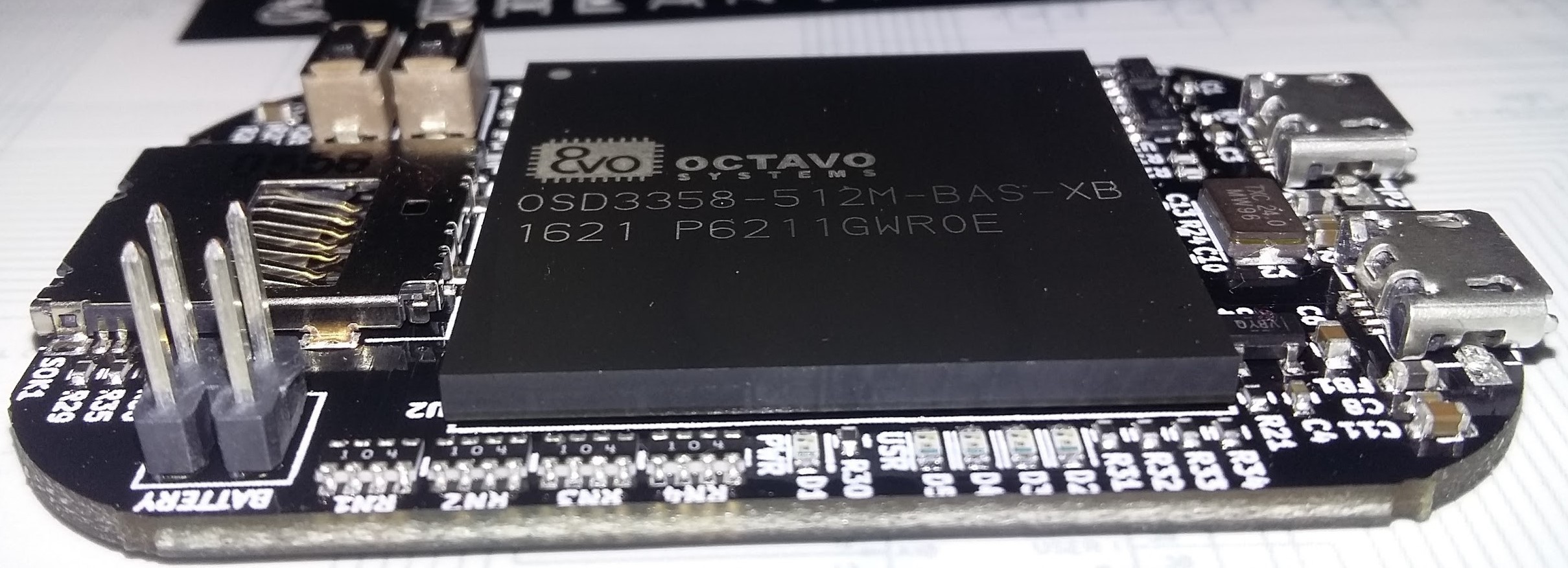
Finally, a request was made that I put all the components on the top side of the board. I had originally put the MicroSD and expansion header on the bottom. Moving everything to the top side makes populating the board simpler (and more cost-effective) because it only takes a single pass through the reflow oven.
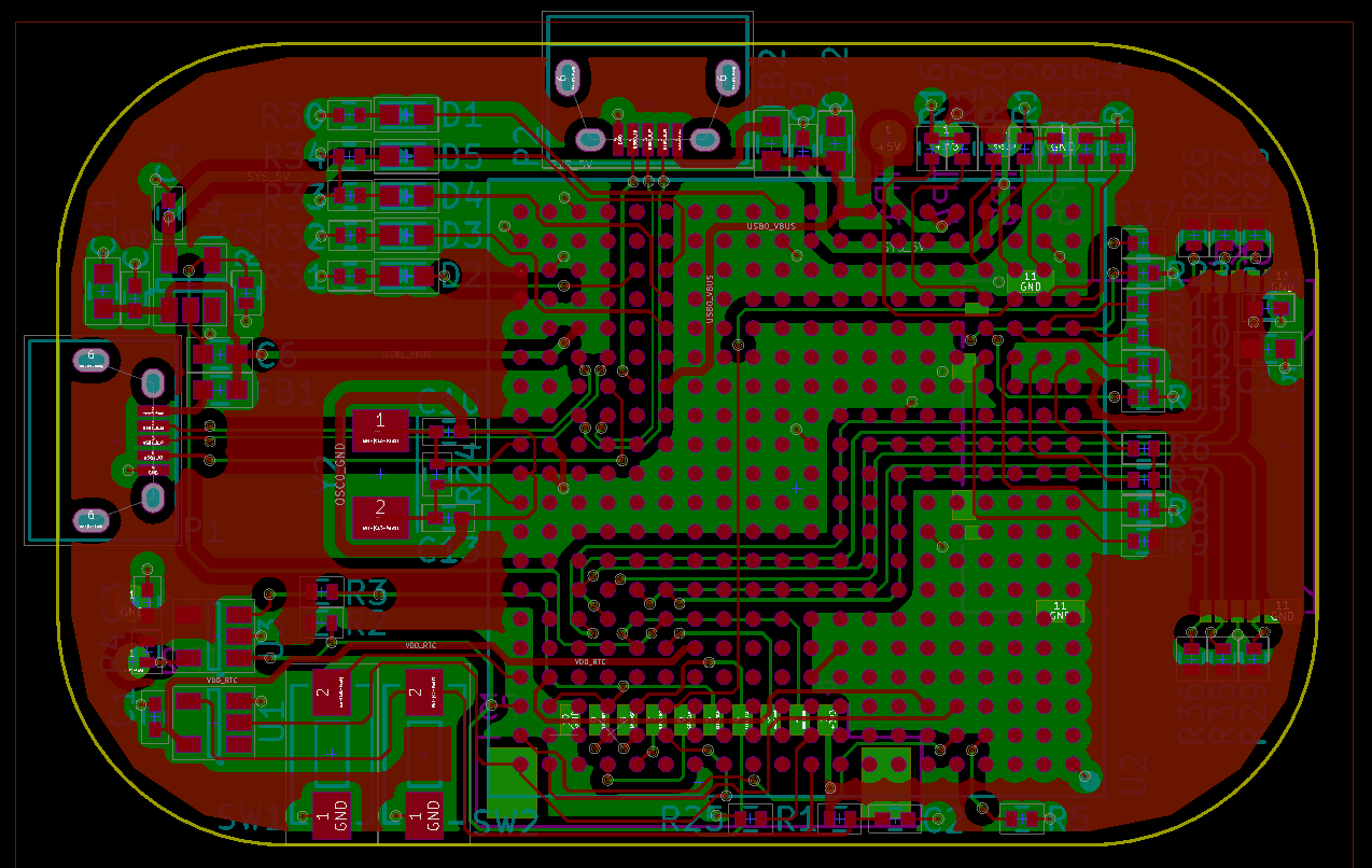 | 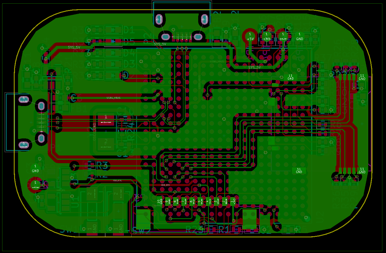 |
With all of this feedback, I decided to pull up all the routing and completely rework the component placement. After some shuffling and part swapping, the placement was consolidated to a single side and sent off for approval. As a bonus, the new placement even left enough room for a battery header to be added. Once the component layout was approved, the second pass at routing commenced.
I wanted to route this layout in 2 layers as well. However, it was becoming difficult and I still had concerns about the USB impedance. After a few attempts, I made the executive decision to switch to 4 layers. This calmed my concerns about the USB routing. USB has strict requirements for trace impedance which cannot be easily met with a standard thickness 2 layer PCB.
Switching to 4 layers was not a problem because I was using KiCAD. Unlike the free version of Eagle CAD, KiCAD has no layer and board size restrictions.
Once the routing was complete, the design was posted for another review.
 |  |
 |  |
Somewhere in the middle of the process of routing the board, I created a Hackaday.io page to document the design in progress and get more community feedback. Hackaday.io is a relatively new forum for aspiring hackers to share projects that they are working on. Hackaday.io is hosted by Hackaday.com, known for its daily hacker blog started in 2004. The PocketBone Hackaday.io page is a good place to find the latest status of the project.
Building The Board
With the routing completed, I started working with Drew Fustini to get the PCB’s from OSH Park, a low-cost batch PCB manufacturer. Drew works at OSH Park and the got me the first PCBs free of charge. In exchange, I created a special edition with the OSH Park logo on it. OSH Park is known for their high-quality purple PCBs and reasonable low volume pricing. While in Portland for the Embedded Linux Conference I had the pleasure of visiting OSH Park to pick up the boards in person.
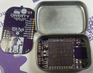
The original and OSH Park version of the design were posted publicly to OSH Park’s site for anyone who would like to order the boards and attempt assembly.
Meanwhile, Jason Kridner took initiative and put in a turn-key order of the PCBs assembly with Circuithub. He sent me one so I could finish testing everything out.
 |  |
Board Bring Up
The first prototype assemblies worked without issue! The latest Debian image from Beagleboard.org supports the PocketBone thanks to the work done by Robert C. Nelson and Jason. Robert, another Beagleboard.org board member, is the driving force behind the Debian images provided on all of the Beagleboard products.
All that was required was the initial EEPROM programming and the board was ready to go. Once the EEPROM was programmed I plugged it in and voilà!
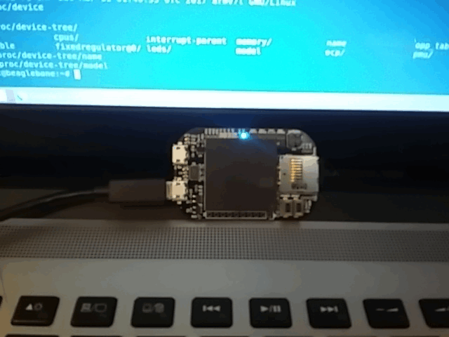
That is it. A Linux PC the size of a Mini-Altoids tin. All of the board designs are freely shared on the Circuithub site for anyone to order.
What’s Next
In the upcoming weeks, I will be attempting to hand-assemble one of these. See my follow up post for details on how the hand assembly went.
I would like to thank Jason, Drew, and Alex for the idea and support along the way.

5 thoughts on “PocketBone: The Linux Computer that Fits in a Mini-Altoids Tin – Designed in KiCad – Featuring the OSD3358”
Technos says:
September 28, 2017 at 6:58 amWhile this is truly an achievement, after briefly scanning the datasheet for the OSD3358 it appears that the current requirement ranges from 1.3 to 2 amps. That seems contradictory for such a small device. I am sure at least half of that is taken up by the USB controller requirements. Which leads to a conclusion (for me at least) that working with such small devices USB controllers are simply incompatible with a future big IoT roll out, and a newer, lower powered peripheral system is needed. Secondly, it is apparent to me that something like the PocketBone probably can not use more than 75 ma to be truly effective in an IoT environment, For a board that comes close, look at TI’s TS-4200 board that consumes .5 Watt, versus PocketBone’s apparent 5 to 10 Watts. It feels like when they ship the PocketBone they need to throw in a couple of shares to the local power company as well!
Not meant as a criticism, just the observation that the future might belong to low power as much as it does small size.
Greg Sheridan says:
September 28, 2017 at 8:32 amThanks for your comment. For clarification the OSD335x does not require 2A of power. What the data sheet is showing you is that the power supply integrated into the device can support up to 2A of power that can be used to power other things in a system. If you are just using the OSD335x and nothing else it will draw significantly less.
Please see our Power App note for more detail on the actual power consumption of the device.
Comments are closed.